 58
58
ASRock Radeon RX 7900 XTX Taichi Review
Test Setup »High-resolution PCB Pictures
These pictures are for the convenience of volt modders and people who would like to see all the finer details on the PCB. Feel free to link back to us and use these in your articles, videos or forum posts.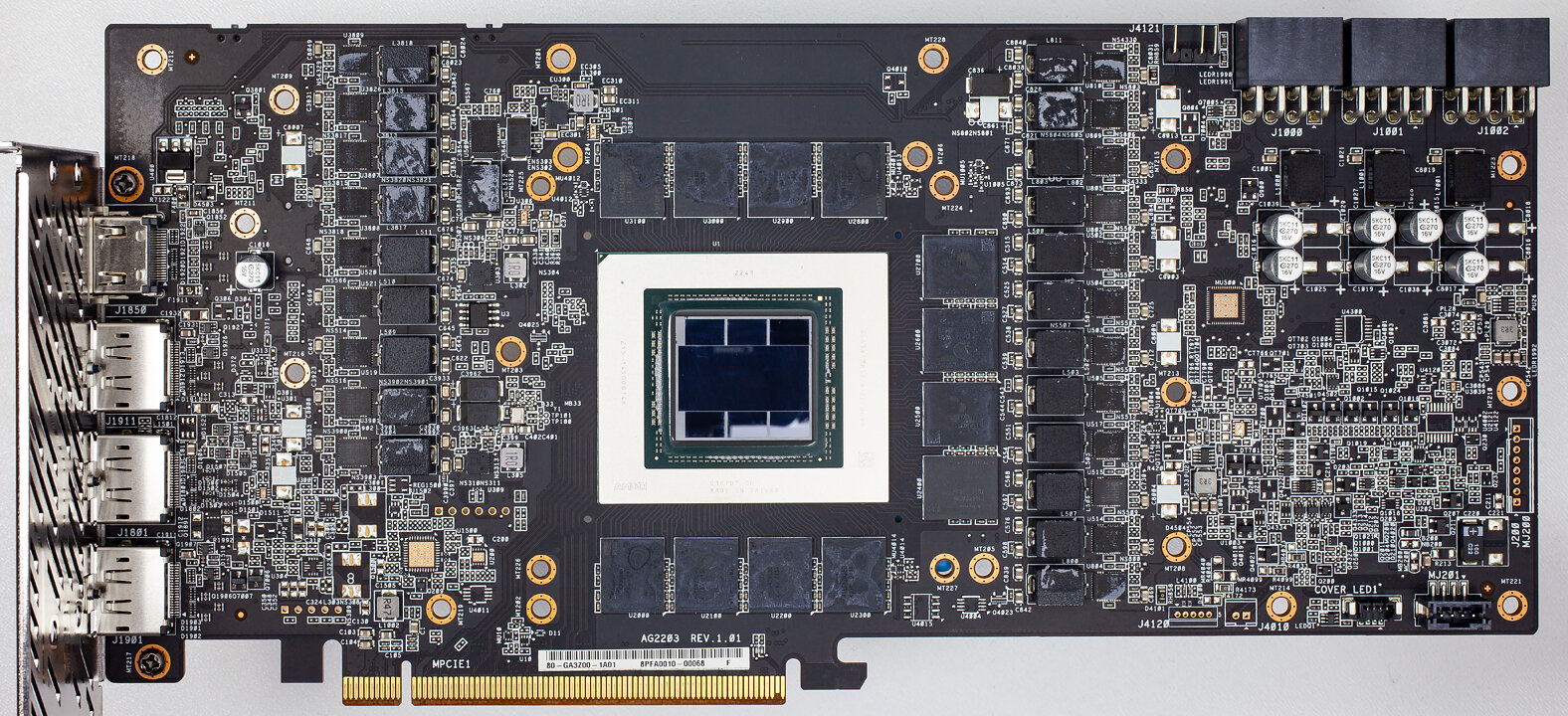

High-resolution versions are also available (front, back).
Circuit Board (PCB) Analysis
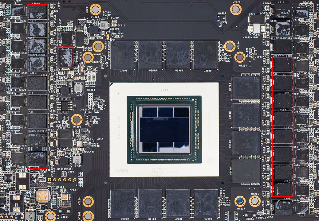

GPU voltage is a 18-phase design, managed by a Monolithic Power Systems MP2857 controller.
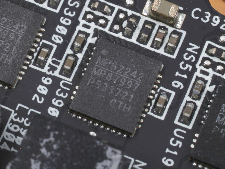
Monolithic MP87997 DrMOS components are used for GPU voltage; they are rated for 70 A of current each.
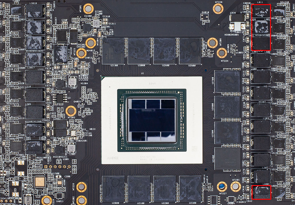
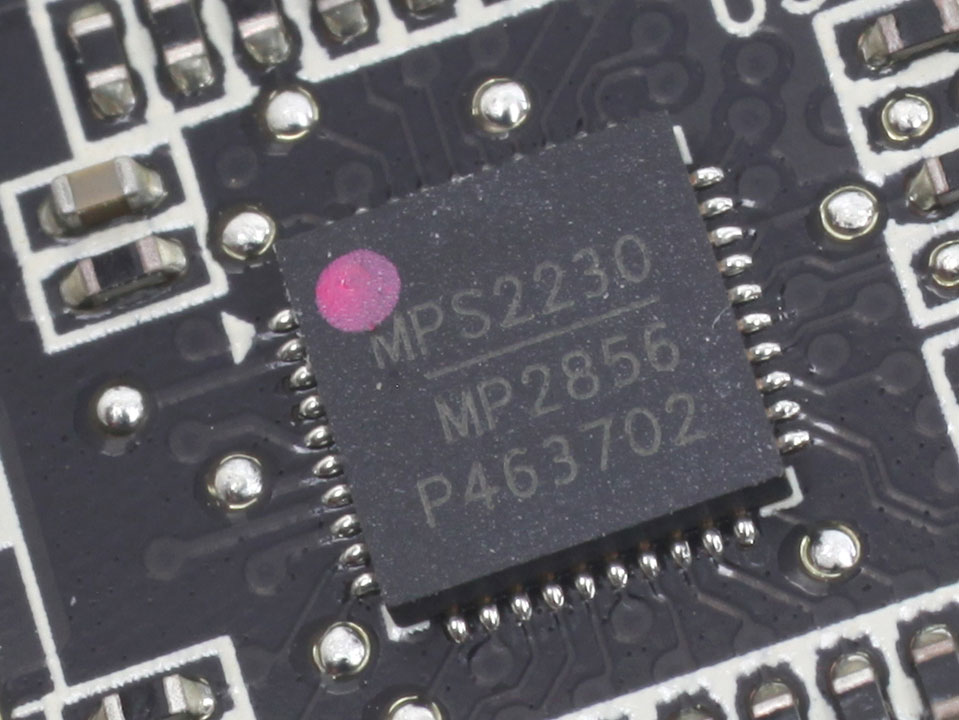
Memory voltage is a four-phase design, managed by a Monolithic Power Systems MP2856 controller.
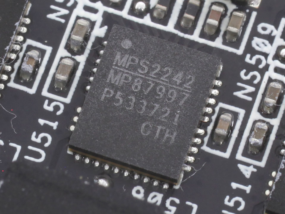
For memory, Monolithic MP87997 DrMOS with a 70 A rating are used again.
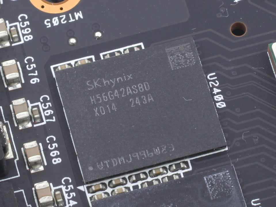
The GDDR6 memory chips are made by Hynix and carry the model number H56G42AS8DX-014. They are specified to run at 2500 MHz (20 Gbps effective).
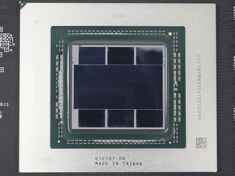
AMD's new Navi 31 graphics processor is the world's first GPU that uses a chiplet architecture. Note the large die in the center, called "GCD," graphics compute die, which houses the compute units, it is surrounded by six smaller "MCD," memory cache dies, that contain one memory controller interface and one slice of cache each. While they look similar, the MCDs are not HBM chips. The MCDs are fabricated on a 6 nm process at TSMC Taiwan with a die size of 36.6 mm² each, the GCD is fabricated using TSMC's 5 nanometer node, with a die size of 300 mm². The combined transistor count of the GPU is 57.7 billion.
Apr 18th, 2024 20:23 EDT
change timezone
Latest GPU Drivers
New Forum Posts
- MSI Z790 owners - be careful, the screw can crack the chipset (4)
- Should the CDPR make the Fallout 5 instead? (12)
- Is it possible that the atmosphere is losing less of its "shield" capabilities due to more and more jets/rockets puncturing it daily? (24)
- Cinebench crashed my PC. My Wi-Fi stopped working, and I keep getting a "Please wait" screen when I boot up my PC. (1)
- Do you use Linux? (226)
- TPU's Nostalgic Hardware Club (18452)
- WX9100 Power mods - help w/ powerplay tables (107)
- XFX RX560 1024 shaders 16 CU 4GB from Aliexpress (5)
- TPU's WCG/BOINC Team (34419)
- Have you got pie today? (16310)
Popular Reviews
- Horizon Forbidden West Performance Benchmark Review - 30 GPUs Tested
- PowerColor Radeon RX 7900 GRE Hellhound Review
- Fractal Design Terra Review
- Corsair 2000D Airflow Review
- Minisforum EliteMini UM780 XTX (AMD Ryzen 7 7840HS) Review
- Creative Pebble X Plus Review
- Thermalright Phantom Spirit 120 EVO Review
- FiiO KB3 HiFi Mechanical Keyboard Review - Integrated DAC/Amp!
- ASUS GeForce RTX 4090 STRIX OC Review
- NVIDIA GeForce RTX 4090 Founders Edition Review - Impressive Performance
Controversial News Posts
- Sony PlayStation 5 Pro Specifications Confirmed, Console Arrives Before Holidays (109)
- NVIDIA Points Intel Raptor Lake CPU Users to Get Help from Intel Amid System Instability Issues (102)
- US Government Wants Nuclear Plants to Offload AI Data Center Expansion (98)
- Windows 10 Security Updates to Cost $61 After 2025, $427 by 2028 (82)
- Developers of Outpost Infinity Siege Recommend Underclocking i9-13900K and i9-14900K for Stability on Machines with RTX 4090 (82)
- TechPowerUp Hiring: Reviewers Wanted for Motherboards, Laptops, Gaming Handhelds and Prebuilt Desktops (71)
- Intel Realizes the Only Way to Save x86 is to Democratize it, Reopens x86 IP Licensing (70)
- AMD Zen 5 Execution Engine Leaked, Features True 512-bit FPU (63)