 63
63
ASUS GeForce RTX 3080 Noctua OC Review - Just Wow
(63 Comments) »Introduction
ASUS and Noctua are easily two of the most respectable brands in the PC component industry. Back in 2021, the company started a collaboration that brought Noctua's expertise in designing high-quality cooling solutions, including fans, and the ASUS wizardry at building top-notch graphics cards together. I've reviewed the ASUS GeForce RTX 3070 Noctua OC in October 2021, was impressed, and begged ASUS for more. Today, that wish comes true, and I have the honor of reviewing the ASUS GeForce RTX 3080 Noctua OC.

It appears that things went well with the RTX 3070 Noctua, and the two companies thus decided on their next project—the RTX 3080, which makes total sense. The card offers performance a tier higher than the RTX 3070 and comes at a higher selling point, which absorbs some of the cost of the new cooler design.
Based on the 8 nm "GA102" silicon, the GeForce RTX 3080 more than doubles the number of unified shaders over the previous-generation RTX 2080. It packs 8,704 CUDA cores, 68 RT cores, and 272 Tensor cores. The memory amount has been increased by 25%, to 10 GB, as has the memory bus width, to 320-bit. NVIDIA and Micron Technology have innovated a whole new memory standard for the GeForce 30 Series, which they call GDDR6X. This memory operates at a data rate of 19 Gbps and has NVIDIA hit memory bandwidth levels of 760 GB/s.
ASUS designed a custom cooling solution for the RTX 3080 Noctua and paired it with the battle-tested PCB design of the RTX 3080 TUF. Physically, this big card takes up four slots, which shouldn't be a problem considering SLI is dead and nearly all people only have one PCIe card installed—the graphics card. In terms of clocks, the ASUS Noctua comes with a small bump in boost clocks, up to 1785 MHz from the NVIDIA baseline frequency of 1710 MHz. According to ASUS, the retail price of the RTX 3080 Noctua OC will be $950, quite a reasonable incresae over the $900 price point the RTX 3080 currently sells for.
| Price | Cores | ROPs | Core Clock | Boost Clock | Memory Clock | GPU | Transistors | Memory | |
|---|---|---|---|---|---|---|---|---|---|
| RTX 2080 Ti | $720 | 4352 | 88 | 1350 MHz | 1545 MHz | 1750 MHz | TU102 | 18600M | 11 GB, GDDR6, 352-bit |
| RTX 3070 | $630 | 5888 | 96 | 1500 MHz | 1725 MHz | 1750 MHz | GA104 | 17400M | 8 GB, GDDR6, 256-bit |
| RTX 3070 Ti | $700 | 6144 | 96 | 1575 MHz | 1770 MHz | 1188 MHz | GA104 | 17400M | 8 GB, GDDR6X, 256-bit |
| RX 6800 | $720 | 3840 | 96 | 1815 MHz | 2105 MHz | 2000 MHz | Navi 21 | 26800M | 16 GB, GDDR6, 256-bit |
| RX 6800 XT | $800 | 4608 | 128 | 2015 MHz | 2250 MHz | 2000 MHz | Navi 21 | 26800M | 16 GB, GDDR6, 256-bit |
| RTX 3080 | $900 | 8704 | 96 | 1440 MHz | 1710 MHz | 1188 MHz | GA102 | 28000M | 10 GB, GDDR6X, 320-bit |
| ASUS RTX 3080 Noctua | $950 | 8704 | 96 | 1440 MHz | 1785 MHz | 1188 MHz | GA102 | 28000M | 10 GB, GDDR6X, 320-bit |
| RTX 3080 Ti | $1,150 | 10240 | 112 | 1365 MHz | 1665 MHz | 1188 MHz | GA102 | 28000M | 12 GB, GDDR6X, 384-bit |
| RX 6900 XT | $1,000 | 5120 | 128 | 2015 MHz | 2250 MHz | 2000 MHz | Navi 21 | 26800M | 16 GB, GDDR6, 256-bit |
| RX 6950 XT | $1,100 | 5120 | 128 | 2100 MHz | 2310 MHz | 2250 MHz | Navi 21 | 26800M | 16 GB, GDDR6, 256-bit |
| RTX 3090 | $1,350 | 10496 | 112 | 1395 MHz | 1695 MHz | 1219 MHz | GA102 | 28000M | 24 GB, GDDR6X, 384-bit |
| RTX 3090 Ti | $1,950 | 10752 | 112 | 1560 MHz | 1950 MHz | 1313 MHz | GA102 | 28000M | 24 GB, GDDR6X, 384-bit |
Packaging


The Card
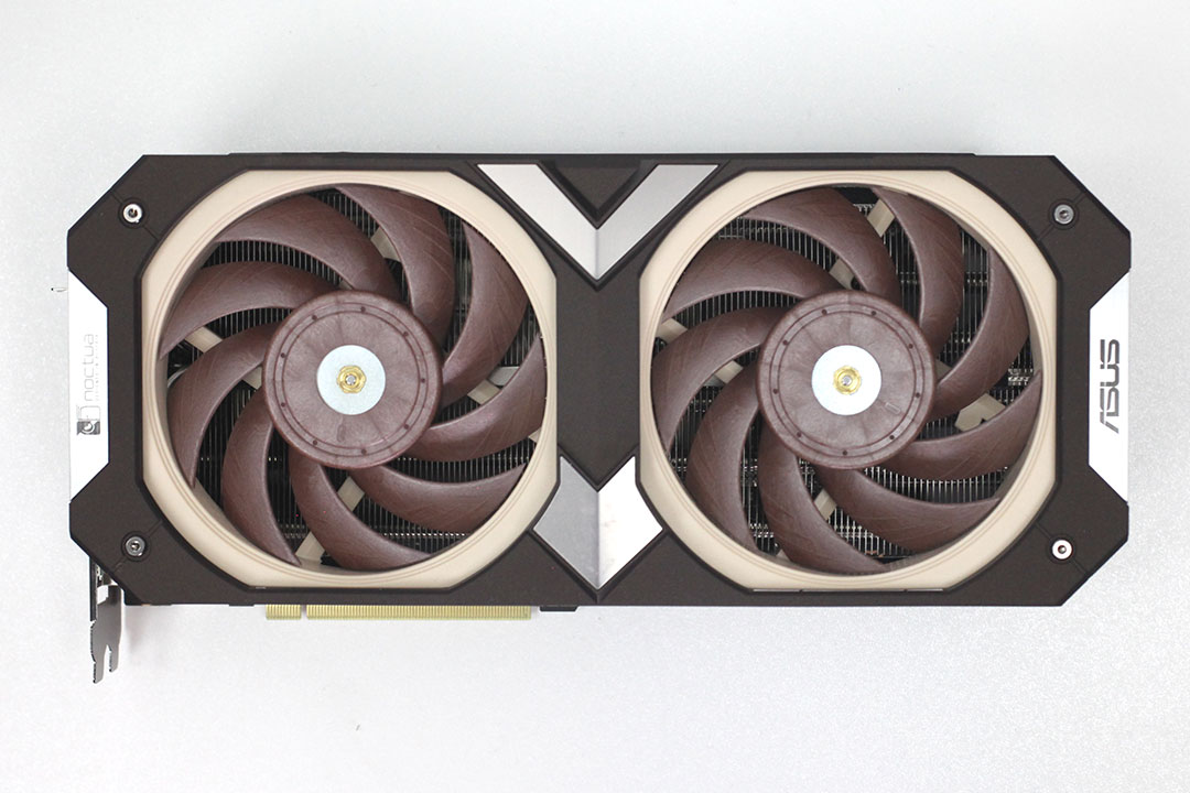

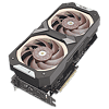
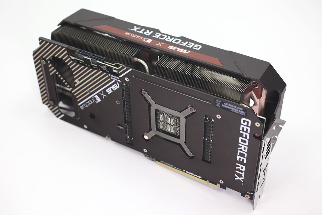
Even at a first glance, this card screams "Noctua." Both companies were wise to keep the tan-and-brown color theme of the Noctua brand on the fans, although I'm sure a lot of people will hate on the color. Visually, the card looks nearly identical to the RTX 3070 Noctua I reviewed October last year, which is fine. On the back, you'll find a metal backplate with a cutout to let airflow through; here, the color theme is black with yellow and gold highlights.

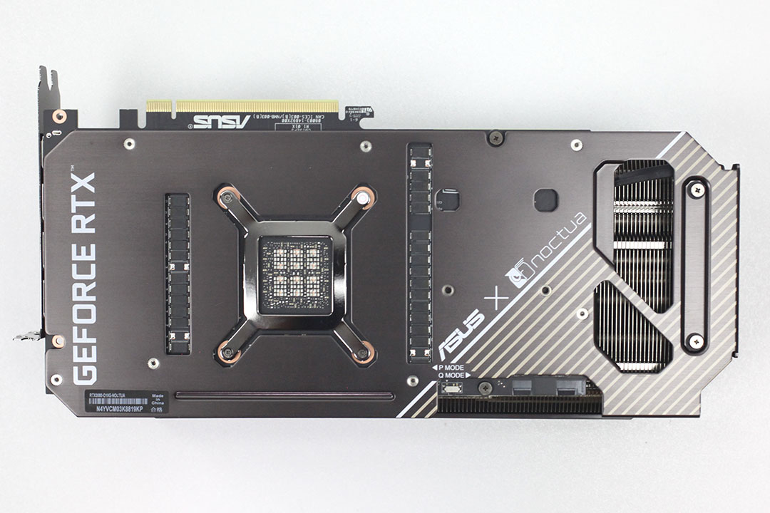
Dimensions of the card are 31.0 x 14.5 cm, and it weighs 1,845 g.
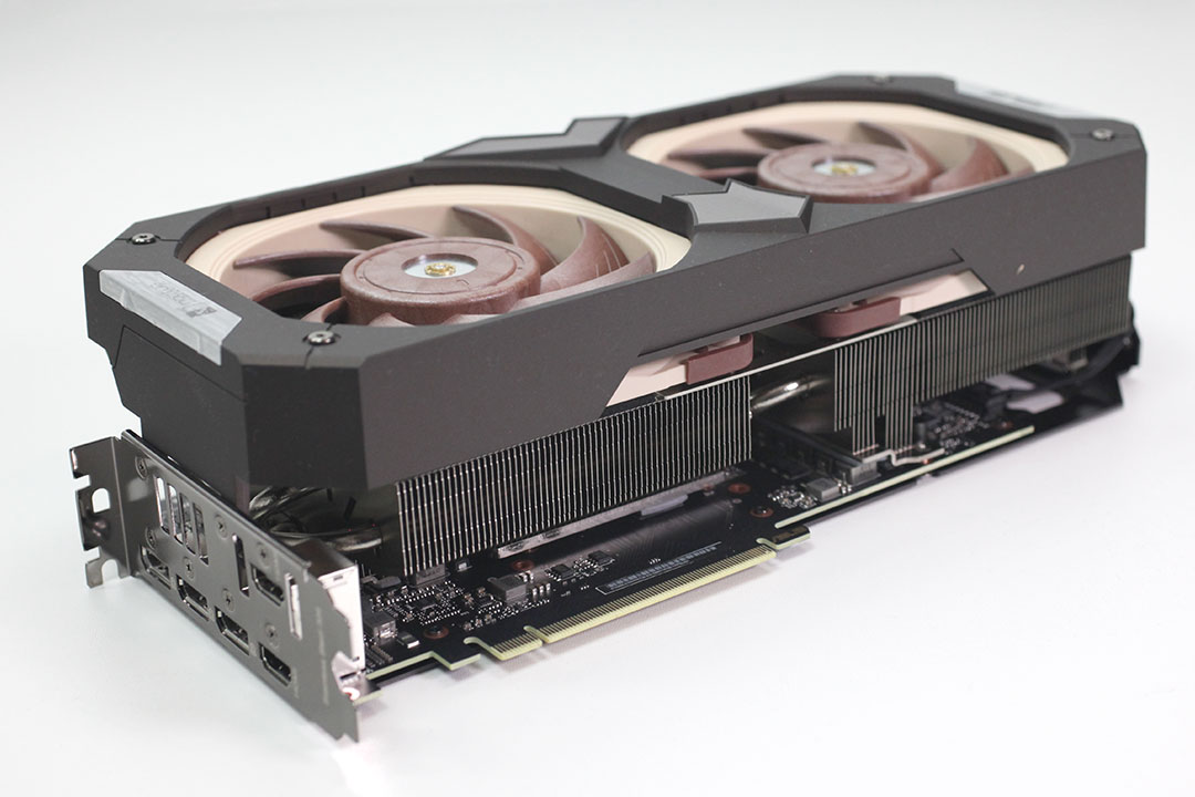
Installation requires four PCIe slots of space in your system. This is a really thick card due to the full-width fans. SLI is dead, so I'm not seeing any issues here space-wise.

Display connectivity includes three standard DisplayPort 1.4, and two HDMI 2.1.

The card has two 8-pin power inputs. This configuration is rated for up to 375 W of power draw. This area also houses the dual BIOS switch, which lets you switch from the default "quiet" BIOS to a "performance" BIOS with a more aggressive fan curve. As we'll see later in our testing, there's no reason to switch to the other BIOS as operating temperatures are excellent even with the quiet BIOS.

The GeForce RTX 3080 does not support SLI.
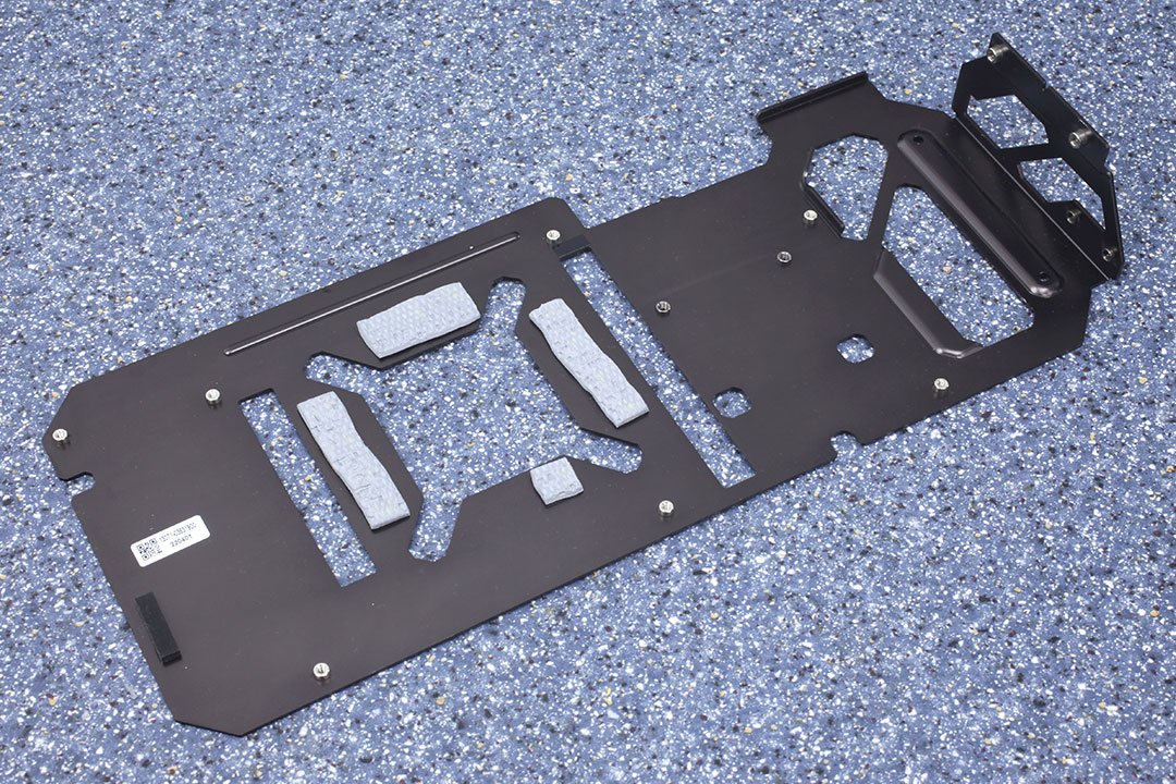
Teardown


The ASUS thermal solution, which is stronger than the one on the RTX 3070 Noctua, uses six heatpipes and a large heatsink to keep the card cool. VRMs and memory chips are cooled by the main heatsink,too.

The fans are standard full-size NF-A12x25 120 mm fans. This makes swapping out the fans in the future for different models or replacing a broken fan incredibly easy; they even use standard 4-pin connectors.
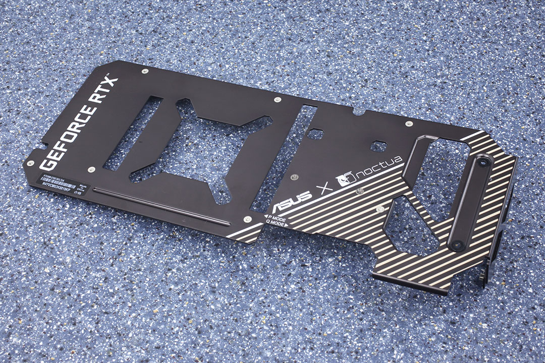
The backplate is made out of metal and protects the card against damage during handling and installation.
High-resolution PCB Pictures
These pictures are for the convenience of volt modders and people who would like to see all the finer details on the PCB. Feel free to link back to us and use these in your articles, videos or forum posts.

High-res versions are also available (front, back).
Circuit Board (PCB) Analysis


The ASUS RTX 3080 TUF Gaming OC uses a pair of UPI uP9512R 8-phase VRM controllers, which put out a 16-phase VRM for the GPU.

ASUS is using Vishay Siliconix SiC654 DrMOS components for the GPU VRM, which are rated for 50 A.
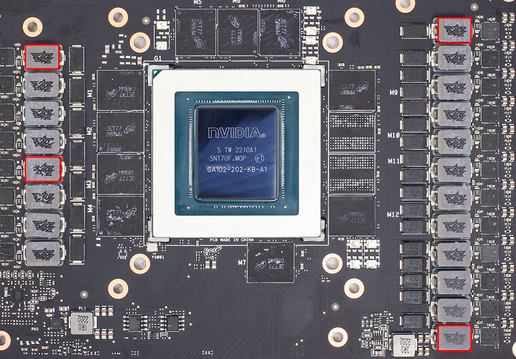

The memory power is a 4-phase setup managed by a uP9512S controller.

For memory, the same Vishay SiC654 DrMOS chips are used as on the GPU VRM.
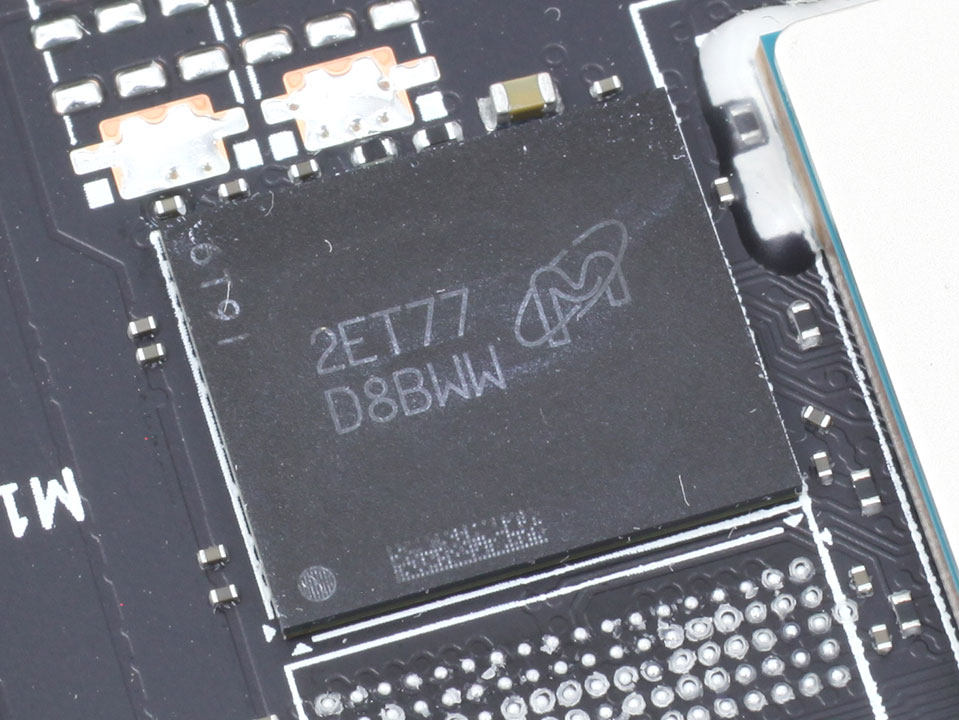
The GDDR6X memory chips are made by Micron and carry the model number D8BWW, which decodes to MT61K256M32JE-19G:T. They are specified to run at 1188 MHz (19 Gbps GDDR6X effective).

NVIDIA's GA102 graphics processor is the company's second Ampere architecture chip; the first one targeted at GeForce gamers. It is produced on a 8 nanometer process at Samsung and has a transistor count of 28 billion with a die size of 628 mm².
Our Patreon Silver Supporters can read articles in single-page format.
May 2nd, 2024 18:13 EDT
change timezone
Latest GPU Drivers
New Forum Posts
- Folding Pie and Milestones!! (9015)
- Problem with a brand new 7700xt. Display stays black and the PC beeps 1 long 2 short after starting it. Need help! (31)
- Are all software/scheduling issues with e-cores fixed on Intel 12th to 14th Gen - Willing to give hybrid ach a chance now (93)
- Technical Issues - TPU Main Site & Forum (2024) (51)
- best budget freindly 5.1 soundbars in 2024 (4)
- PYPrime 2.x free Memory benchmark. let's see those daily Memory OC performances. (43)
- TPU's Nostalgic Hardware Club (18493)
- FINAL FANTASY XIV: Dawntrail Official Benchmark (75)
- 7900 XTX Seriously lacking (106)
- Bad temps? (13)
Popular Reviews
- Ugreen NASync DXP4800 Plus Review
- ASRock NUC BOX-155H (Intel Core Ultra 7 155H) Review
- Montech Sky Two GX Review
- HYTE THICC Q60 240 mm AIO Review
- Upcoming Hardware Launches 2023 (Updated Feb 2024)
- MOONDROP x Crinacle DUSK In-Ear Monitors Review - The Last 5%
- Team Group T-Force Vulcan ECO DDR5-6000 32 GB CL38 Review
- AMD Ryzen 7 7800X3D Review - The Best Gaming CPU
- Thermalright Phantom Spirit 120 EVO Review
- ASUS Radeon RX 7900 GRE TUF OC Review
Controversial News Posts
- Intel Statement on Stability Issues: "Motherboard Makers to Blame" (228)
- Windows 11 Now Officially Adware as Microsoft Embeds Ads in the Start Menu (164)
- Sony PlayStation 5 Pro Specifications Confirmed, Console Arrives Before Holidays (117)
- AMD's RDNA 4 GPUs Could Stick with 18 Gbps GDDR6 Memory (114)
- NVIDIA Points Intel Raptor Lake CPU Users to Get Help from Intel Amid System Instability Issues (106)
- AMD "Strix Halo" Zen 5 Mobile Processor Pictured: Chiplet-based, Uses 256-bit LPDDR5X (103)
- AMD Ryzen 9 7900X3D Now at a Mouth-watering $329 (102)
- TechPowerUp Hiring: Reviewers Wanted for Motherboards, Laptops, Gaming Handhelds and Prebuilt Desktops (93)