 37
37
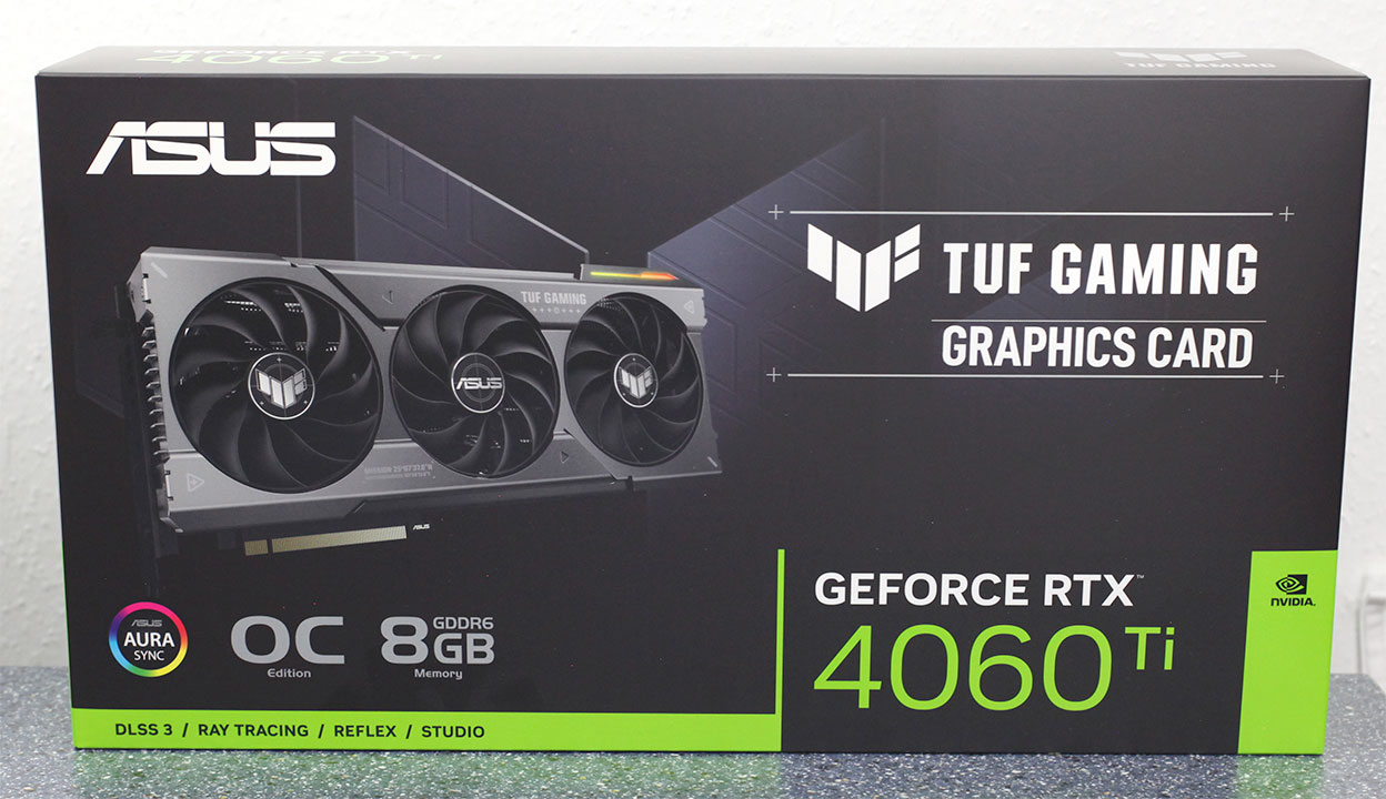
ASUS GeForce RTX 4060 Ti TUF OC Review
(37 Comments) »Introduction
ASUS TUF Gaming GeForce RTX 4060 Ti OC is a serious-looking, factory-overclocked, custom-design rendition of NVIDIA's latest entry to the mid-range. The new RTX 4060 Ti is designed for maxed out gaming at 1080p, including with ray tracing. You can take advantage of features such as DLSS 3 Frame Generation to even play at higher resolutions such as 1440p on supported games, with fairly high settings. Firmly rooted in the GeForce RTX 40-series, and based on the Ada Lovelace graphics architecture, the RTX 4060 Ti offers all of the new-generation features, and since the GPU uses the latest 5 nm foundry process, you can expect some of the best performance/Watt for gaming graphics.

The GeForce RTX 4060 Ti debuts the new 5 nm AD106 silicon to the desktop segment, which it nearly maxes out, enabling 34 out of 36 streaming multiprocessors (SM), which work out to 4,352 CUDA cores, 34 RT cores, 136 Tensor cores, 136 TMUs, and 48 ROPs. 8 GB is still the standard memory size for the RTX 4060 Ti (a 16 GB variant is coming this July), however, compared to its predecessor, the RTX 3060 Ti, NVIDIA has narrowed the memory bus width to 128-bit. The company is using faster 18 Gbps GDDR6 memory chips, but the real secret-sauce is at the architecture-level, where NVIDIA has enlarged the on-die L2 cache by eight times compared to the GA104 silicon powering the RTX 3060 Ti. This reduces the GPU's memory round-trips for its most frequent data access, by anywhere between 40-60%, allowing NVIDIA to slim the memory interface. The GeForce Ada graphics architecture debuts the 3rd generation of NVIDIA RTX, the company's groundbreaking technology that combines real-time ray traced elements such as lighting, shadows, reflections, global illumination, and motion-blur, with conventional raster 3D graphics, to significantly increase realism.
The ASUS TUF Gaming RTX 4060 Ti uses a large triple-slot cooling solution, with a design focus on low noise. This big cooler should make short work of the GPU's low heat output—its TGP is just rated at 160 W, which is also why the company opted for a single 8-pin PCIe power connector. The cooler is designed to make it easy to maintain the fans and heatsink, without having to reapply the TIM. You also get some handy features such as dual-BIOS, letting you switch to a Quiet BIOS that runs a more relaxed fan curve. The company is pricing the card at $460, a steep 15% step up from the $400 NVIDIA MSRP.
| Price | Cores | ROPs | Core Clock | Boost Clock | Memory Clock | GPU | Transistors | Memory | |
|---|---|---|---|---|---|---|---|---|---|
| RTX 2060 | $180 | 1920 | 48 | 1365 MHz | 1680 MHz | 1750 MHz | TU106 | 10800M | 6 GB, GDDR6, 192-bit |
| RX Vega 64 | $320 | 4096 | 64 | 1247 MHz | 1546 MHz | 953 MHz | Vega 10 | 12500M | 8 GB, HBM2, 2048-bit |
| RX 5700 XT | $180 | 2560 | 64 | 1605 MHz | 1755 MHz | 1750 MHz | Navi 10 | 10300M | 8 GB, GDDR6, 256-bit |
| RTX 3050 | $260 | 2560 | 32 | 1552 MHz | 1777 MHz | 1750 MHz | GA106 | 12000M | 8 GB, GDDR6, 128-bit |
| RTX 2070 | $230 | 2304 | 64 | 1410 MHz | 1620 MHz | 1750 MHz | TU106 | 10800M | 8 GB, GDDR6, 256-bit |
| RX 6600 | $210 | 1792 | 64 | 2044 MHz | 2491 MHz | 1750 MHz | Navi 23 | 11060M | 8 GB, GDDR6, 128-bit |
| RTX 3060 | $300 | 3584 | 48 | 1320 MHz | 1777 MHz | 1875 MHz | GA106 | 12000M | 12 GB, GDDR6, 192-bit |
| RTX 4060 | $300 | 3072 | 32 | 1830 MHz | 2460 MHz | 2125 MHz | AD107 | unknown | 8 GB, GDDR6, 128-bit |
| RX 6600 XT | $250 | 2048 | 64 | 2359 MHz | 2589 MHz | 2000 MHz | Navi 23 | 11060M | 8 GB, GDDR6, 128-bit |
| Arc A750 | $250 | 3584 | 112 | 2050 MHz | N/A | 2000 MHz | ACM-G10 | 21700M | 8 GB, GDDR6, 256-bit |
| Arc A770 | $290 | 4096 | 128 | 2100 MHz | N/A | 2187 MHz | ACM-G10 | 21700M | 16 GB, GDDR6, 256-bit |
| RTX 2080 | $260 | 2944 | 64 | 1515 MHz | 1710 MHz | 1750 MHz | TU104 | 13600M | 8 GB, GDDR6, 256-bit |
| RTX 3060 Ti | $320 | 4864 | 80 | 1410 MHz | 1665 MHz | 1750 MHz | GA104 | 17400M | 8 GB, GDDR6, 256-bit |
| RTX 4060 Ti | $400 | 4352 | 48 | 2310 MHz | 2535 MHz | 2250 MHz | AD106 | 22900M | 8 GB, GDDR6, 128-bit |
| ASUS RTX 4060 Ti TUF | $460 | 4352 | 48 | 2310 MHz | 2625 MHz | 2250 MHz | AD106 | 22900M | 8 GB, GDDR6, 128-bit |
| RX 6700 XT | $320 | 2560 | 64 | 2424 MHz | 2581 MHz | 2000 MHz | Navi 22 | 17200M | 12 GB, GDDR6, 192-bit |
| RTX 2080 Ti | $400 | 4352 | 88 | 1350 MHz | 1545 MHz | 1750 MHz | TU102 | 18600M | 11 GB, GDDR6, 352-bit |
| RTX 3070 | $350 | 5888 | 96 | 1500 MHz | 1725 MHz | 1750 MHz | GA104 | 17400M | 8 GB, GDDR6, 256-bit |
| RTX 3070 Ti | $420 | 6144 | 96 | 1575 MHz | 1770 MHz | 1188 MHz | GA104 | 17400M | 8 GB, GDDR6X, 256-bit |
Architecture
The Ada graphics architecture heralds the third generation of the NVIDIA RTX technology, an effort toward increasing the realism of game visuals by leveraging real-time ray tracing, without the enormous amount of compute power required to draw purely ray-traced 3D graphics. This is done by blending conventional raster graphics with ray traced elements such as reflections, lighting, and global illumination, to name a few. The 3rd generation of RTX introduces the new higher IPC "Ada" CUDA core, 3rd generation RT core, 4th generation Tensor core, and the new Optical Flow Processor, a component that plays a key role in generating new frames without involving the GPU's main graphics rendering pipeline.


The GeForce Ada graphics architecture driving the RTX 4060 Ti leverages the TSMC 5 nm EUV foundry process to increase transistor counts. At the heart of this GPU is the new AD106 silicon, with a fairly high transistor count of 22.9 billion, which is almost double that of the previous-generation GA106, and still about 30% more than the GA104. The GPU features a generationally narrower PCI-Express 4.0 x8 host interface, and a 128-bit wide GDDR6 memory interface. This is causing some controversy, and we'll present NVIDIA's explanation below. The Optical Flow Accelerator (OFA) is an independent top-level component. The chip features one NVENC and one NVDEC unit.
The essential component hierarchy is similar to past generations of NVIDIA GPUs. The AD106 silicon features 3 Graphics Processing Clusters (GPCs), each of these has all the SIMD and graphics rendering machinery, and is a small GPU in its own right. Each GPC shares a raster engine (geometry processing components) and two ROP partitions (each with eight ROP units). The GPC of the AD106 contains five Texture Processing Clusters (TPCs), the main number-crunching machinery. Each of these has two Streaming Multiprocessors (SM), and a Polymorph unit. Each SM contains 128 CUDA cores across four partitions. Half of these CUDA cores are pure-FP32; while the other half is capable of FP32 or INT32. The SM retains concurrent FP32+INT32 math processing capability. The SM also contains a 3rd generation RT core, four 4th generation Tensor cores, some cache memory, and four TMUs. There are 12 SM per GPC, so 1,536 CUDA cores, 48 Tensor cores, and 12 RT cores; per GPC. There are three such GPCs, which add up to 4,608 CUDA cores, 144 TMUs, 144 Tensor Cores, and 36 RT cores. Each GPC contributes 16 ROPs, so there are 48 ROPs on the silicon. The RTX 4060 Ti is carved out of the AD106 by disabling one TPC worth 256 CUDA cores. This yields 4,352 CUDA cores, 136 Tensor cores, 34 RT cores, and 136 TMUs. The ROP count is untouched at 48, as is the on-die L2 cache, which is 32 MB in size.

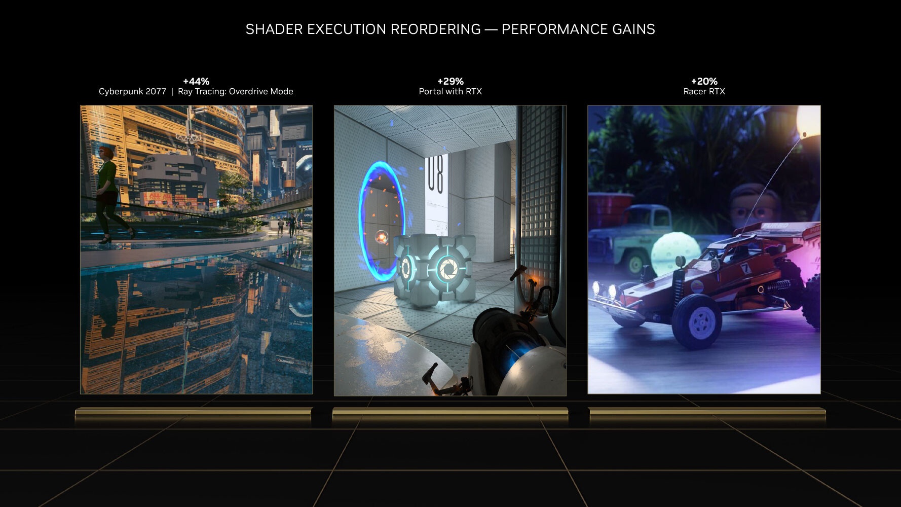
The 3rd generation RT core accelerates the most math-intensive aspects of real-time ray tracing, including BVH traversal. Displaced micro-mesh engine is a revolutionary feature introduced with the new 3rd generation RT core. Just as mesh shaders and tessellation have had a profound impact on improving performance with complex raster geometry, allowing game developers to significantly increase geometric complexity; DMMs is a method to reduce the complexity of the bounding-volume hierarchy (BVH) data-structure, which is used to determine where a ray hits geometry. Previously, the BVH had to capture even the smallest details to properly determine the intersection point. Ada's ray tracing architecture also receives a major performance uplift from Shader Execution Reordering (SER), a software-defined feature that requires awareness from game-engines, to help the GPU reorganize and optimize worker threads associated with ray tracing.

The BVH now needn't have data for every single triangle on an object, but can represent objects with complex geometry as a coarse mesh of base triangles, which greatly simplifies the BVH data structure. A simpler BVH means less memory consumed and helps to greatly reduce ray tracing CPU load, because the CPU only has to generate a smaller structure. With older "Ampere" and "Turing" RT cores, each triangle on an object had to be sampled at high overhead, so the RT core could precisely calculate ray intersection for each triangle. With Ada, the simpler BVH, plus the displacement maps can be sent to the RT core, which is now able to figure out the exact hit point on its own. NVIDIA has seen 11:1 to 28:1 compression in total triangle counts. This reduces BVH compile times by 7.6x to over 15x, in comparison to the older RT core; and reducing its storage footprint by anywhere between 6.5 to 20 times. DMMs could reduce disk- and memory bandwidth utilization, utilization of the PCIe bus, as well as reduce CPU utilization. NVIDIA worked with Simplygon and Adobe to add DMM support for their tool chains.


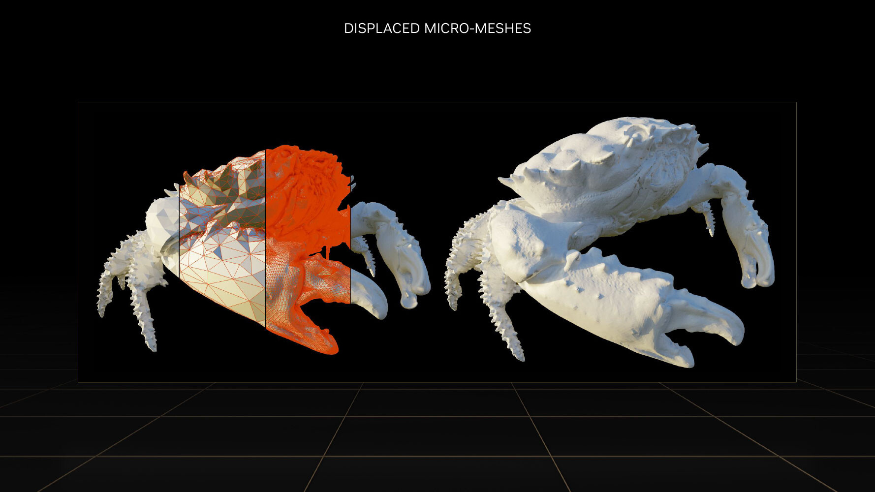
Opacity Micro Meshes (OMM) is a new feature introduced with Ada to improve rasterization performance, particularly with objects that have alpha (transparency data). Most low-priority objects in a 3D scene, such as leaves on a tree, are essentially rectangles with textures on the leaves where the transparency (alpha) creates the shape of the leaf. RT cores have a hard time intersecting rays with such objects, because they're not really in the shape that they appear (they're really just rectangles with textures that give you the illusion of shape). Previous-generation RT cores had to have multiple interactions with the rendering stage to figure out the shape of a transparent object, because they couldn't test for alpha by themselves.

This has been solved by using OMMs. Just as DMMs simplify geometry by creating meshes of micro-triangles; OMMs create meshes of rectangular textures that align with parts of the texture that aren't alpha, so the RT core has a better understanding of the geometry of the object, and can correctly calculate ray intersections. This has a significant performance impact on shading performance in non-RT applications, too. Practical applications of OMMs aren't just low-priority objects such as vegetation, but also smoke-sprites and localized fog. Traditionally there was a lot of overdraw for such effects, because they layered multiple textures on top of each other, that all had to be fully processed by the shaders. Now only the non-opaque pixels get executed—OMMs provide a 30 percent speedup with graphics buffer fill-rates, and a 10 percent impact on frame-rates.


DLSS 3 introduces a revolutionary new feature that promises a doubling in frame-rate at comparable quality, it's called AI frame-generation. While it has all the features of DLSS 2 and its AI super-resolution (scaling up a lower-resolution frame to native resolution with minimal quality loss); DLSS 3 can generate entire frames simply using AI, without involving the graphics rendering pipeline. Later in the article, we will show you DLSS 3 in action.


Every alternating frame with DLSS 3 is hence AI-generated, without being a replica of the previous rendered frame. This is possible only on the Ada graphics architecture, because of a hardware component called the optical flow accelerator (OFA), which assists in predicting what the next frame could look like, by creating what NVIDIA calls an optical flow-field. OFA ensures that the DLSS 3 algorithm isn't confused by static objects in a rapidly-changing 3D scene (such as a race sim). The process heavily relies on the performance uplift introduced by the FP8 math format of the 4th generation Tensor core. A third key ingredient of DLSS 3 is Reflex. By reducing the rendering queue to zero, Reflex plays a vital role in ensuring that frame-times with DLSS 3 are at an acceptable level, and a render-queue doesn't confuse the upscaler. A combination of OFA and the 4th Gen Tensor core is why the Ada architecture is required to use DLSS 3, and why it won't work on older architectures.
Ada Rebalanced Memory Subsystem

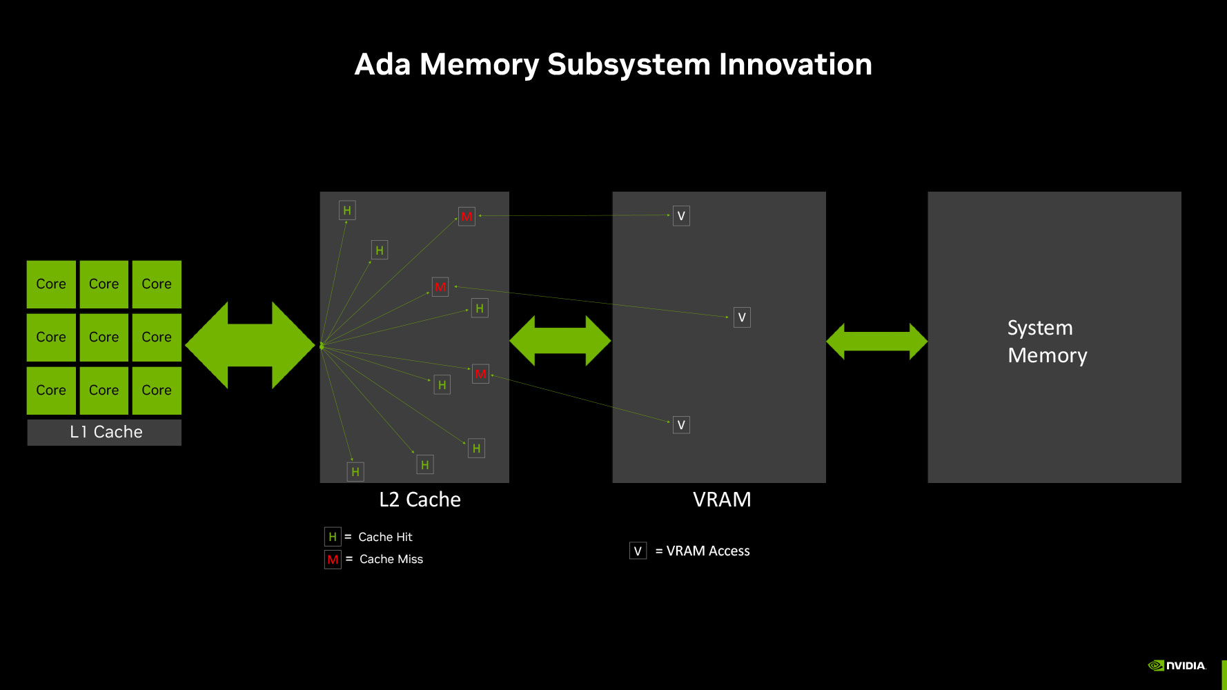
The previous-generation GeForce RTX 3060 Ti featured a 256-bit wide GDDR6 memory interface driving its 8 GB of 14 Gbps-rated GDDR6 memory (448 GB/s memory bandwidth), which has caused some controversy with the new RTX 4060 Ti using a narrower 128-bit wide memory interface to drive 8 GB of 18 Gbps memory (288 GB/s bandwidth). With the new Ada Lovelace graphics architecture, NVIDIA has tried to re-balance the memory sub-system such that there's dependence on larger on-die caches, allowing NVIDIA to narrow down the GPU's GDDR6 memory interface. The obvious benefit of this to NVIDIA is reduced costs, let's make no mistake about it, but NVIDIA maintains that this isn't a big problem for the GPU.
The last-level cache, or L2 cache, of NVIDIA Ada GPUs is anywhere between 8-10 times larger than the ones on the previous-generation Ampere GPUs. The AD106 silicon powering the RTX 4060 Ti has a 32 MB L2 cache, compared to the 4 MB of the GA104 silicon powering the RTX 3060 Ti. NVIDIA illustrated an example of how a the larger on-die LLC reduces video memory pressure (trips to GDDR6) by anywhere between 40% to 60% on the same GPU, by soaking up a larger number of memory access requests by the shaders.
The L2 cache is unified victim cache to the GPU's various GPCs and their local TPCs. Data that isn't hot enough (frequently accessed enough) to be resident on the small L1 caches of the SM, is ejected to the L2 cache, and depending on its heat, pushed to the GDDR6 video memory. The L2 cache is an order of magnitude faster than than video memory in terms of latency, and so having frequently-accessed data reside there offers a considerable benefit.

As we mentioned earlier from NVIDIA's claims, this re-balancing of the memory sub-system between the on-die LLC and video memory lowers the GPU's access to the latter by as much as 60%, which means the GPU can make do with a narrower 128-bit wide GDDR6 memory bus. NVIDIA has used generationally faster 18 Gbps memory chips in the RTX 4060 Ti. NVIDIA developed a new means of presenting the memory bandwidth that takes into account the contribution of the L2 cache, its hit-rate, and the consequent reduction in video memory traffic. While the memory bandwidth of the RTX 4060 Ti is 288 GB/s, NVIDIA claims that its "effective bandwidth" is 554 GB/s (23% higher than the 448 GB/s memory bandwidth of the RTX 3060 Ti). It's interesting to point out that NVIDIA has used "effective bandwidth" figures in the past to highlight its lossless memory compression technologies, but has never been this vocal about it.
Packaging

The Card


ASUS TUF Gaming RTX 4060 Ti OC uses the latest generation of the company's muscular-looking TUF Gaming cooling solution, which uses a large aluminium fin-stack heatsink that's ventilated by a trio of fans. The card certainly looks like it's from a segment above when installed in your case.


Dimensions of the card are 30.0 x 14.0 cm, and it weighs 1088 g.

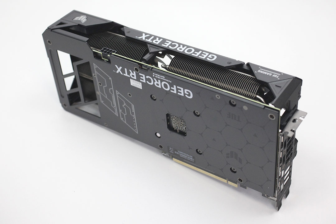
Installation requires three slots in your system.

Display connectivity includes three standard DisplayPort 1.4a ports and one HDMI 2.1a (same as Ampere).
The new 8th Gen NVENC now accelerates AV1 encoding, besides HEVC. You also get an "optical flow accelerator" unit that is able to calculate intermediate frames for videos, to smooth playback. The same hardware unit is used for frame generation in DLSS 3.
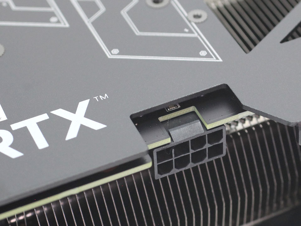
ASUS opted for a single 8-pin PCIe power connector, this configuration is good for up to 225 W.

This little switch lets you select between the default "Performance" P-BIOS, and the Quiet Q-BIOS, which runs a more relaxed fan curve for reduced noise.
Teardown


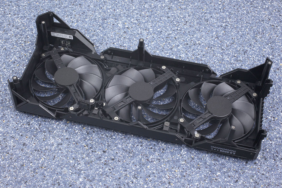
The cooler shroud and the main heatsink are held to the PCB and backplate with separate sets of screws. What this means is that the cooler shroud comes off, without disturbing the heatsink and its TIM or thermal pads, so you can easily clean the fans and the heatsink without much effort.


ASUS uses a set of nickel-plated copper base-plates, which are connected to two aluminium fin-stacks on either ends of heatpipes.

Four heatpipes move heat away from the GPU surface to the heatsink.


ASUS is using a sturdy metal backplate that's folded on the edges, so it works to counteract PCB bending over time.
High-resolution PCB Pictures
These pictures are for the convenience of volt modders and people who would like to see all the finer details on the PCB. Feel free to link back to us and use these in your articles, videos or forum posts.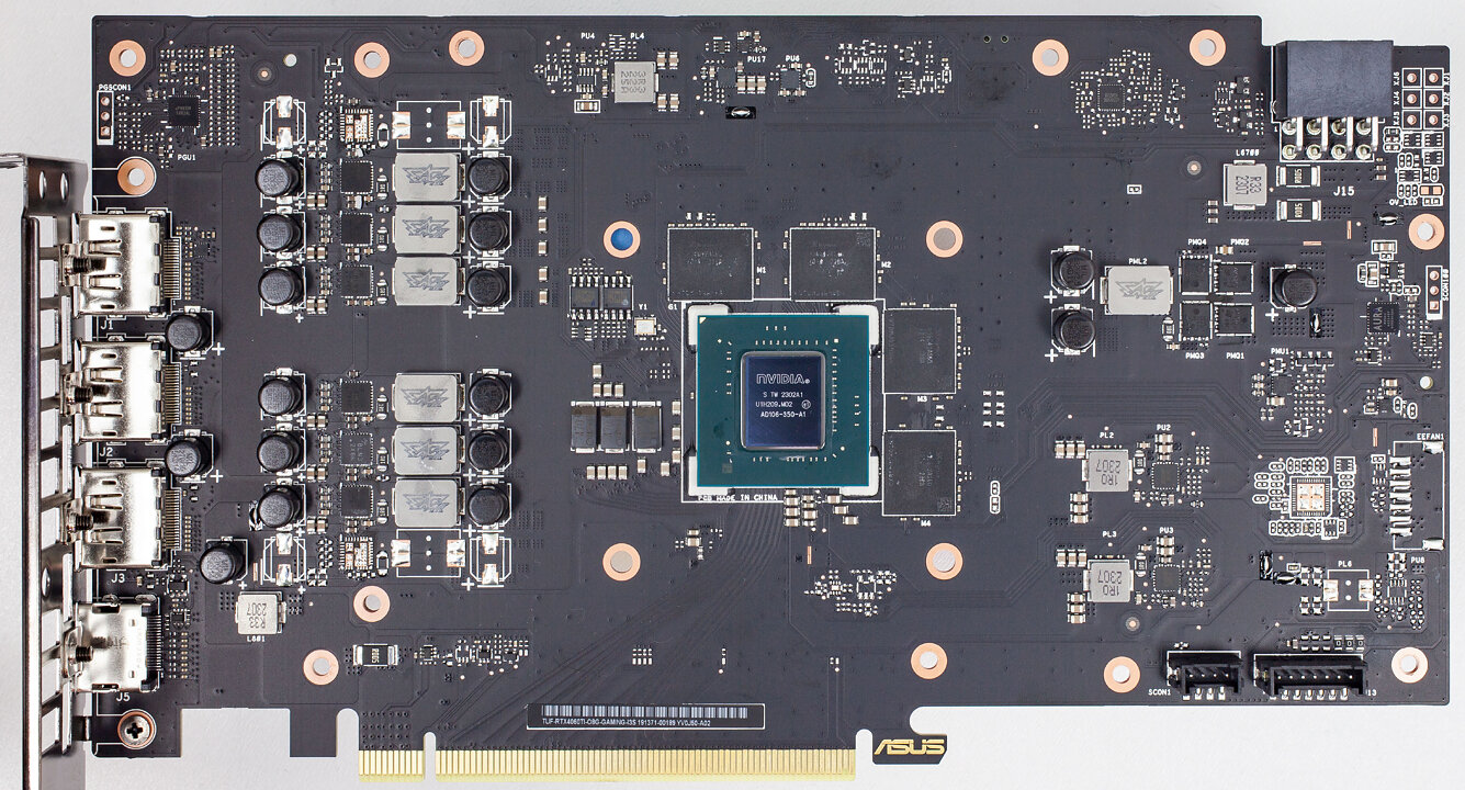

High-resolution versions are also available (front, back).
Our Patreon Silver Supporters can read articles in single-page format.
May 9th, 2024 13:44 EDT
change timezone
Latest GPU Drivers
New Forum Posts
- Your way of cooling your PC? (87)
- Only some humans can see refresh rates faster than others, I am one of those humans. (234)
- TPU's Nostalgic Hardware Club (18504)
- Battery swap for cyberpower UPS (66)
- Last game you purchased? (275)
- Current Sales, Bundles, Giveaways (10231)
- What's a good option for a digital touchless thermometer? (17)
- Epic Games launcher's ridiculous CPU usage (33)
- AM5 boot times improve RADICALLY with memory context restore enabled (1)
- Microsoft butchering Xbox Studios (26)
Popular Reviews
- CHERRY XTRFY M64 Pro Review
- Corsair iCUE Link RX120 RGB 120 mm Fan Review
- Bykski CPU-XPR-C-I CPU Water Block Review - Amazing Value!
- Finalmouse UltralightX Review
- Upcoming Hardware Launches 2023 (Updated Feb 2024)
- Corsair MP700 Pro SE 4 TB Review
- AMD Ryzen 7 7800X3D Review - The Best Gaming CPU
- Cougar Hotrod Royal Gaming Chair Review
- ASUS Radeon RX 7900 GRE TUF OC Review
- Meze Audio LIRIC 2nd Generation Closed-Back Headphones Review
Controversial News Posts
- Intel Statement on Stability Issues: "Motherboard Makers to Blame" (262)
- AMD to Redesign Ray Tracing Hardware on RDNA 4 (206)
- Windows 11 Now Officially Adware as Microsoft Embeds Ads in the Start Menu (167)
- NVIDIA to Only Launch the Flagship GeForce RTX 5090 in 2024, Rest of the Series in 2025 (144)
- Sony PlayStation 5 Pro Specifications Confirmed, Console Arrives Before Holidays (119)
- AMD's RDNA 4 GPUs Could Stick with 18 Gbps GDDR6 Memory (114)
- NVIDIA Points Intel Raptor Lake CPU Users to Get Help from Intel Amid System Instability Issues (106)
- AMD Ryzen 9 7900X3D Now at a Mouth-watering $329 (104)