 37
37
ASUS GeForce RTX 4070 Super TUF OC Review
Pictures & Teardown »Architecture
The Ada graphics architecture heralds the third generation of the NVIDIA RTX technology, an effort toward increasing the realism of game visuals by leveraging real-time ray tracing, without the enormous amount of compute power required to draw purely ray-traced 3D graphics. This is done by blending conventional raster graphics with ray traced elements such as reflections, lighting, and global illumination, to name a few. The 3rd generation of RTX introduces the new higher IPC "Ada" CUDA core, 3rd generation RT core, 4th generation Tensor core, and the new Optical Flow Processor, a component that plays a key role in generating new frames without involving the GPU's main graphics rendering pipeline. The GeForce Ada graphics architecture driving the RTX 4070 SUPER leverages the TSMC 5 nm EUV foundry process to increase transistor counts.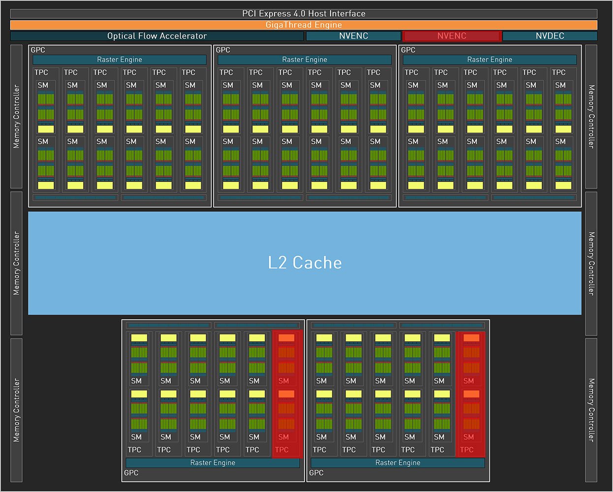


The new GeForce RTX 4070 SUPER is based on the same AD104 silicon as the original RTX 4070 and the RTX 4070 Ti. The former is heavily cut down from the silicon, while the latter maxes it out. The RTX 4070 SUPER doesn't strike a middle-ground between the two, but rather tilts close to the RTX 4070 Ti. Out of the 60 streaming multiprocessors physically present on the silicon, the RTX 4070 SUPER gets a substantial 56, or 93% of the available shaders. In comparison, the RTX 4070 only enabled 46 SM, or just 76% of them. Besides increasing the SM count, NVIDIA gave the RTX 4070 SUPER the full 48 MB of L2 cache present on the silicon, compared to just 36 MB on the RTX 4070; and the full ROP count of 80, compared to 64 on the RTX 4070. What sets the RTX 4070 SUPER apart from the RTX 4070 Ti is 4 SM worth 512 CUDA cores, the lack of dual NVENC accelerators (the RTX 4070 SUPER has just one of the two NVENC units enabled, just like on the RTX 4070); and a higher power TGP of 285 W on the RTX 4070 Ti, while the RTX 4070 SUPER TGP is set to 225 W. The lower power limits might affect boost frequency residency.
With 56 out of 60 SM enabled, the RTX 4070 SUPER enjoys 7,168 CUDA cores, 224 Tensor cores, 56 RT cores, 224 TMUs, and 80 ROPs. As we mentioned, it gets the full 48 MB of L2 cache, which should make its memory sub-system identical to that of the RTX 4070 Ti—you get 12 GB of 21 Gbps GDDR6X memory across a 192-bit memory bus. We'll explain later how the seemingly narrow memory bus shouldn't worry you.
The component hierarchy of the 5 nm AD104 silicon is similar to that of several past generations of NVIDIA GPUs. It features a PCI-Express 4.0 x16 host interface that supports PCI-Express Resizable BAR; and a 192-bit GDDR6X memory bus that drives its 12 GB of memory. The GigaThread Engine forms the front-end of the GPU as a processor, and controls traffic among the five graphics processing clusters (GPCs). Each of the five GPCs on the AD104 has a Raster Engine with 16 ROPs, and six Texture Processing Clusters (TPCs). Each of these has two Streaming Multiprocessors (SM), and a Polymorph unit. Each SM contains 128 CUDA cores across four partitions. Half of these CUDA cores are pure-FP32; while the other half is capable of FP32 or INT32. The SM retains concurrent FP32+INT32 math processing capability. The SM also contains a 3rd generation RT core, four 4th generation Tensor cores, some cache memory, and four TMUs. With six TPCs per GPC on the AD104, there are a total of 60 SM. NVIDIA carved the RTX 4070 SUPER by disabling two TPCs. The AD104 features two NVENC accelerators, and one NVDEC accelerator. The RTX 4070 Ti has both NVENC units enabled, but the RTX 4070 SUPER, like the RTX 4070, has one of the two NVENC units disabled.
3rd Gen RT Core and Ray Tracing


The 3rd generation RT core accelerates the most math-intensive aspects of real-time ray tracing, including BVH traversal. Displaced micro-mesh engine is a revolutionary feature introduced with the new 3rd generation RT core. Just as mesh shaders and tessellation have had a profound impact on improving performance with complex raster geometry, allowing game developers to significantly increase geometric complexity; DMMs is a method to reduce the complexity of the bounding-volume hierarchy (BVH) data-structure, which is used to determine where a ray hits geometry. Previously, the BVH had to capture even the smallest details to properly determine the intersection point. Ada's ray tracing architecture also receives a major performance uplift from Shader Execution Reordering (SER), a software-defined feature that requires awareness from game-engines, to help the GPU reorganize and optimize worker threads associated with ray tracing.


The BVH now needn't have data for every single triangle on an object, but can represent objects with complex geometry as a coarse mesh of base triangles, which greatly simplifies the BVH data structure. A simpler BVH means less memory consumed and helps to greatly reduce ray tracing CPU load, because the CPU only has to generate a smaller structure. With older "Ampere" and "Turing" RT cores, each triangle on an object had to be sampled at high overhead, so the RT core could precisely calculate ray intersection for each triangle. With Ada, the simpler BVH, plus the displacement maps can be sent to the RT core, which is now able to figure out the exact hit point on its own. NVIDIA has seen 11:1 to 28:1 compression in total triangle counts. This reduces BVH compile times by 7.6x to over 15x, in comparison to the older RT core; and reducing its storage footprint by anywhere between 6.5 to 20 times. DMMs could reduce disk- and memory bandwidth utilization, utilization of the PCIe bus, as well as reduce CPU utilization. NVIDIA worked with Simplygon and Adobe to add DMM support for their tool chains.
Opacity Micro Meshes


Opacity Micro Meshes (OMM) is a new feature introduced with Ada to improve rasterization performance, particularly with objects that have alpha (transparency data). Most low-priority objects in a 3D scene, such as leaves on a tree, are essentially rectangles with textures on the leaves where the transparency (alpha) creates the shape of the leaf. RT cores have a hard time intersecting rays with such objects, because they're not really in the shape that they appear (they're really just rectangles with textures that give you the illusion of shape). Previous-generation RT cores had to have multiple interactions with the rendering stage to figure out the shape of a transparent object, because they couldn't test for alpha by themselves.


This has been solved by using OMMs. Just as DMMs simplify geometry by creating meshes of micro-triangles; OMMs create meshes of rectangular textures that align with parts of the texture that aren't alpha, so the RT core has a better understanding of the geometry of the object, and can correctly calculate ray intersections. This has a significant performance impact on shading performance in non-RT applications, too. Practical applications of OMMs aren't just low-priority objects such as vegetation, but also smoke-sprites and localized fog. Traditionally there was a lot of overdraw for such effects, because they layered multiple textures on top of each other, that all had to be fully processed by the shaders. Now only the non-opaque pixels get executed—OMMs provide a 30 percent speedup with graphics buffer fill-rates, and a 10 percent impact on frame-rates.
DLSS 3 Frame Generation
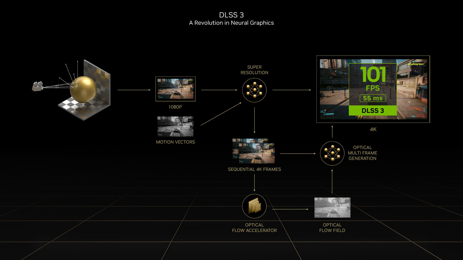

DLSS 3 introduces a revolutionary new feature that promises a doubling in frame-rate at comparable quality, it's called AI frame-generation. Building on DLSS 2 and its AI super-resolution (scaling up a lower-resolution frame to native resolution with minimal quality loss); DLSS 3 can generate entire frames simply using AI, without involving the graphics rendering pipeline, it's also possible to enable frame generation at native resolution without upscaling. Later in the article, we will show you DLSS 3 in action.


Every alternating frame with DLSS 3 is hence AI-generated, without being a replica of the previous rendered frame. This is possible only on the Ada graphics architecture, because of a hardware component called the optical flow accelerator (OFA), which assists in predicting what the next frame could look like, by creating what NVIDIA calls an optical flow-field. OFA ensures that the DLSS 3 algorithm isn't confused by static objects in a rapidly-changing 3D scene (such as a race sim). The process heavily relies on the performance uplift introduced by the FP8 math format of the 4th generation Tensor core. A third key ingredient of DLSS 3 is Reflex. By reducing the rendering queue to zero, Reflex plays a vital role in ensuring that latency with DLSS 3 enabled is at an acceptable level. A combination of OFA and the 4th Gen Tensor core is why the Ada architecture is required to use DLSS 3, and why it won't work on older architectures.
Ada Rebalanced Memory Subsystem


The previous-generation GeForce RTX 3070 Ti featured a 256-bit wide GDDR6 memory interface driving its 8 GB of 19 Gbps-rated GDDR6X memory (608 GB/s bandwidth), while the RTX 4070, RTX 4070 SUPER, and RTX 4070 Ti, use narrower 192-bit interfaces. This is made up for with use of faster 21 Gbps memory speed (504 GB/s). You'll notice that besides the top RTX 4090, every SKU in the RTX 40-series has a generationally narrower memory interface (albeit with faster and larger memory). This shouldn't bother you, and here's why. With the new Ada Lovelace graphics architecture, NVIDIA has tried to re-balance the memory sub-system such that there's dependence on larger on-die caches, allowing NVIDIA to narrow down the GPU's GDDR6 memory interface. The obvious benefit of this to NVIDIA is reduced costs, let's make no mistake about it, but NVIDIA maintains that this isn't a big problem for the GPU.
The last-level cache, or L2 cache, of NVIDIA Ada GPUs is anywhere between 8-10 times larger than the ones on the previous-generation Ampere GPUs. The AD104 silicon powering the RTX 4070 SUPER has a 48 MB L2 cache, compared to the 4 MB of the GA104 silicon powering the RTX 3070 Ti. NVIDIA illustrated an example of how the larger on-die LLC reduces video memory pressure (trips to GDDR6) by anywhere between 40% to 60% on the same GPU, by soaking up a larger number of memory access requests by the shaders.
The L2 cache is unified victim cache to the GPU's various GPCs and their local TPCs. Data that isn't hot enough (frequently accessed enough) to be resident on the small L1 caches of the SM, is ejected to the L2 cache, and depending on its heat, pushed to the GDDR6 video memory. The L2 cache is an order of magnitude faster than than video memory in terms of latency, and so having frequently-accessed data reside there offers a considerable benefit.

As we mentioned earlier from NVIDIA's claims, this re-balancing of the memory sub-system between the on-die LLC and video memory lowers the GPU's access to the latter by as much as 60%, which means the GPU can make do with a narrower 192-bit wide GDDR6X memory bus. NVIDIA has used generationally faster 21 Gbps memory chips in the RTX 4070 SUPER. NVIDIA developed a new means of presenting the memory bandwidth that takes into account the contribution of the L2 cache, its hit-rate, and the consequent reduction in video memory traffic.
May 8th, 2024 16:43 EDT
change timezone
Latest GPU Drivers
New Forum Posts
- Does anyone here overclock their video cards? Is it really worth it? (71)
- What's a good option for a digital touchless thermometer? (1)
- POLL: Can you see the difference past 60fps (gaming/other) (54)
- Arkane Austin and Redfall: what happened? (50)
- Urgent: PC wont turn on with PSU connected to MOBO (27)
- Epic Games launcher's ridiculous CPU usage (30)
- not impressed - nvme vs ssd (70)
- AMD RX 7000 series GPU Owners' Club (1100)
- Your way of cooling your PC? (32)
- High c0% and system idle process (4)
Popular Reviews
- CHERRY XTRFY M64 Pro Review
- Corsair iCUE Link RX120 RGB 120 mm Fan Review
- Finalmouse UltralightX Review
- Bykski CPU-XPR-C-I CPU Water Block Review - Amazing Value!
- Upcoming Hardware Launches 2023 (Updated Feb 2024)
- Cougar Hotrod Royal Gaming Chair Review
- Meze Audio LIRIC 2nd Generation Closed-Back Headphones Review
- AMD Ryzen 7 7800X3D Review - The Best Gaming CPU
- ASRock NUC BOX-155H (Intel Core Ultra 7 155H) Review
- ASUS Radeon RX 7900 GRE TUF OC Review
Controversial News Posts
- Intel Statement on Stability Issues: "Motherboard Makers to Blame" (261)
- AMD to Redesign Ray Tracing Hardware on RDNA 4 (206)
- Windows 11 Now Officially Adware as Microsoft Embeds Ads in the Start Menu (167)
- NVIDIA to Only Launch the Flagship GeForce RTX 5090 in 2024, Rest of the Series in 2025 (142)
- Sony PlayStation 5 Pro Specifications Confirmed, Console Arrives Before Holidays (119)
- AMD's RDNA 4 GPUs Could Stick with 18 Gbps GDDR6 Memory (114)
- NVIDIA Points Intel Raptor Lake CPU Users to Get Help from Intel Amid System Instability Issues (106)
- AMD Ryzen 9 7900X3D Now at a Mouth-watering $329 (104)