 296
296
ASUS GeForce RTX 4070 Ti TUF Review
Test Setup »High-resolution PCB Pictures
These pictures are for the convenience of volt modders and people who would like to see all the finer details on the PCB. Feel free to link back to us and use these in your articles, videos or forum posts.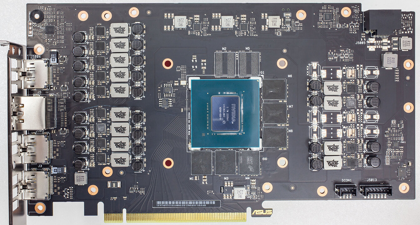
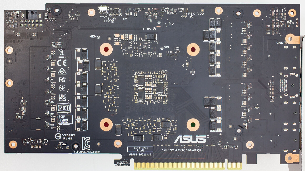
High-resolution versions are also available (front, back).
Circuit Board (PCB) Analysis
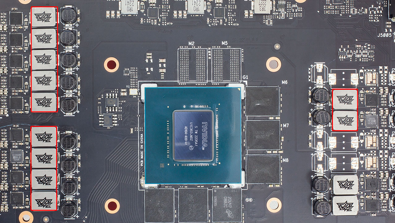

GPU voltage is an 11-phase design, managed by a uPI uP9512R controller.
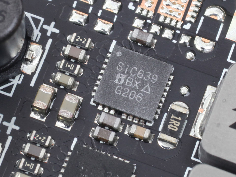
The GPU VRM uses Vishay SiC639 DrMOS components rated for 50 A.


Memory voltage is a two-phase design, managed by a uPI uP9529Q controller.

For memory, Vishay SiC639 DrMOS with a 50 A rating are used again.
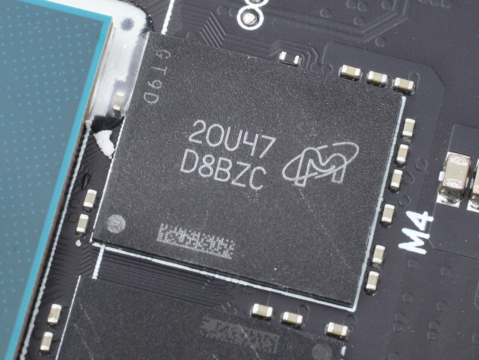
The GDDR6X memory chips are made by Micron and carry the model number D8BZC, which decodes to MT61K512M32KPA-21:U. They are specified to run at 1313 MHz (21 Gbps GDDR6 effective).
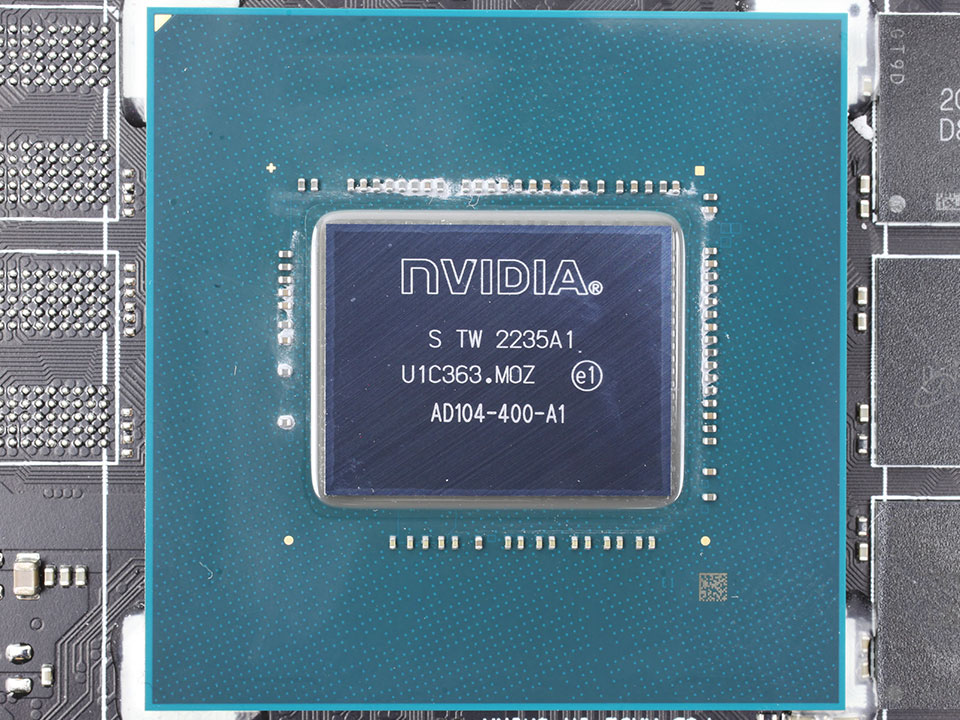
NVIDIA's AD104 graphics processor is the company's third Ada Lovelace GPU. It is built using a 5 nanometer process at TSMC Taiwan, with a transistor count of 35.8 billion and a die size of 295 mm².
Apr 26th, 2024 10:00 EDT
change timezone
Latest GPU Drivers
New Forum Posts
- What are you playing? (20540)
- Secure boot already open help (6)
- Horizontal black lines popping up on my screen? (13)
- Alphacool CORE 1 CPU block - bulging with danger of splitting? (26)
- What's your latest tech purchase? (20351)
- The Official Linux/Unix Desktop Screenshots Megathread (698)
- Which new games will you be buying? (321)
- GoDeal24 Windows 11 Pro 32-bit! (3)
- Old high quality PSU, or semi-old mid-quality PSU? (1)
- Best SSD for system drive (86)
Popular Reviews
- HYTE THICC Q60 240 mm AIO Review
- Alienware Pro Wireless Gaming Keyboard Review
- MOONDROP x Crinacle DUSK In-Ear Monitors Review - The Last 5%
- Upcoming Hardware Launches 2023 (Updated Feb 2024)
- Thermalright Phantom Spirit 120 EVO Review
- ASUS Radeon RX 7900 GRE TUF OC Review
- FiiO K19 Desktop DAC/Headphone Amplifier Review
- RTX 4090 & 53 Games: Ryzen 7 5800X vs Ryzen 7 5800X3D Review
- NVIDIA RTX 4090: 450 W vs 600 W 12VHPWR - Is there any notable performance difference?
- RTX 4090 & 53 Games: Core i9-13900K vs Ryzen 7 5800X3D Review
Controversial News Posts
- Windows 11 Now Officially Adware as Microsoft Embeds Ads in the Start Menu (123)
- Sony PlayStation 5 Pro Specifications Confirmed, Console Arrives Before Holidays (117)
- NVIDIA Points Intel Raptor Lake CPU Users to Get Help from Intel Amid System Instability Issues (106)
- AMD "Strix Halo" Zen 5 Mobile Processor Pictured: Chiplet-based, Uses 256-bit LPDDR5X (101)
- US Government Wants Nuclear Plants to Offload AI Data Center Expansion (98)
- AMD's RDNA 4 GPUs Could Stick with 18 Gbps GDDR6 Memory (90)
- Developers of Outpost Infinity Siege Recommend Underclocking i9-13900K and i9-14900K for Stability on Machines with RTX 4090 (85)
- Windows 10 Security Updates to Cost $61 After 2025, $427 by 2028 (84)