 57
57
ASUS P8P67 PRO Review
BIOS Walkthrough »The Board - A Closer Look

Right above the SATA ports we find the BIOS chip, and much to our pleasant surprise, it's nestled inside a socket that allows easy replacement should the need arise, saving costly RMAs for those that manage to corrupt the BIOS when overclocking. In an effort to prevent that from happening, and ensuring a proper boot no matter what memory is installed, we find a small switch on the upper right corner aptly named "MemOK!". Depressing this switch will begin a set of automatic memory testing that ASUS says guarantees a proper boot, and from our testing, it functions exactly as described.
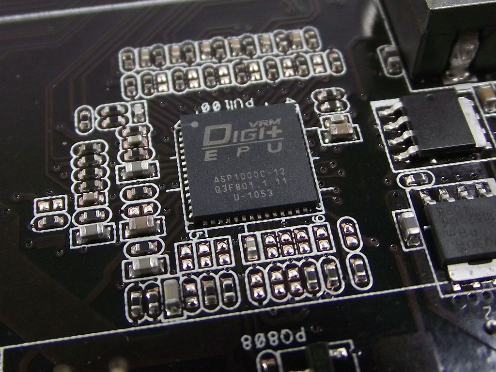

Of course, once the board is booted, several things are now in control of board power, including the new "DIGI+/EPU" chip we found hiding under one of the MOSFET heatsinks. It's partnered with the "TPU" chip, an acronym for Turbo Processing Unit. Of course, EPU stands for something as well, Energy Processing Unit, and together these chips make up the "Dual Intelligent Processers II" solution we find tagged between the expansion slots.
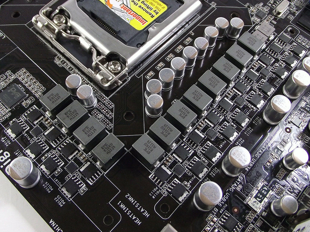

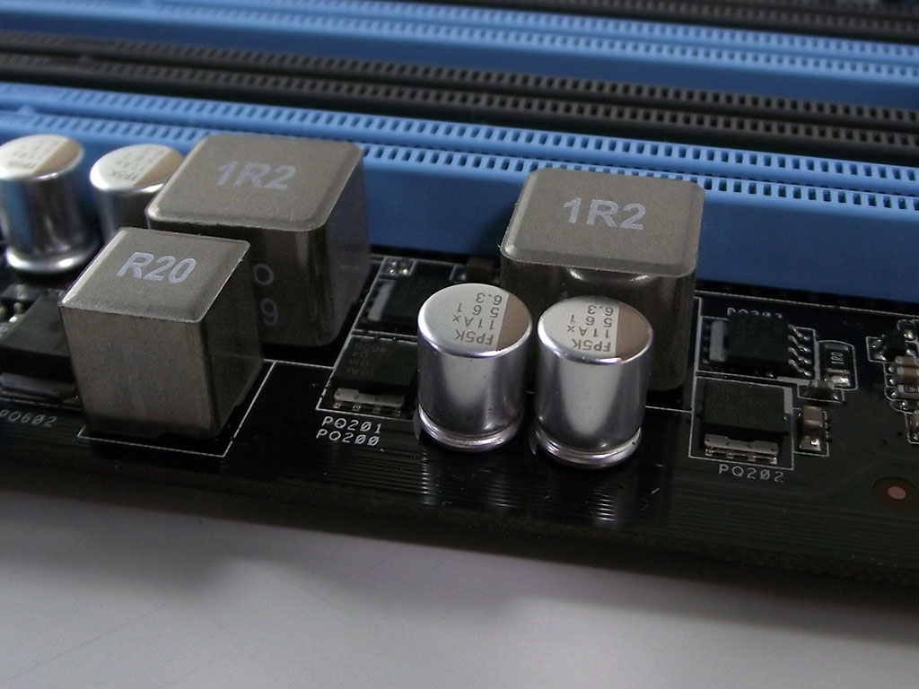
The CPU VRM itself, with the heatsinks removed, reveals to be comprised of many different parts, in a traditional ASUS power design seen on many boards through the years, although updated with newer components that together match the Intel VRD12 specification. You can see two phases that terminate into an encased ferrite choke in the second picture, and in the third picture you'll see that each of the two DIMM power phases is similarly equipped, although terminated with different chokes.
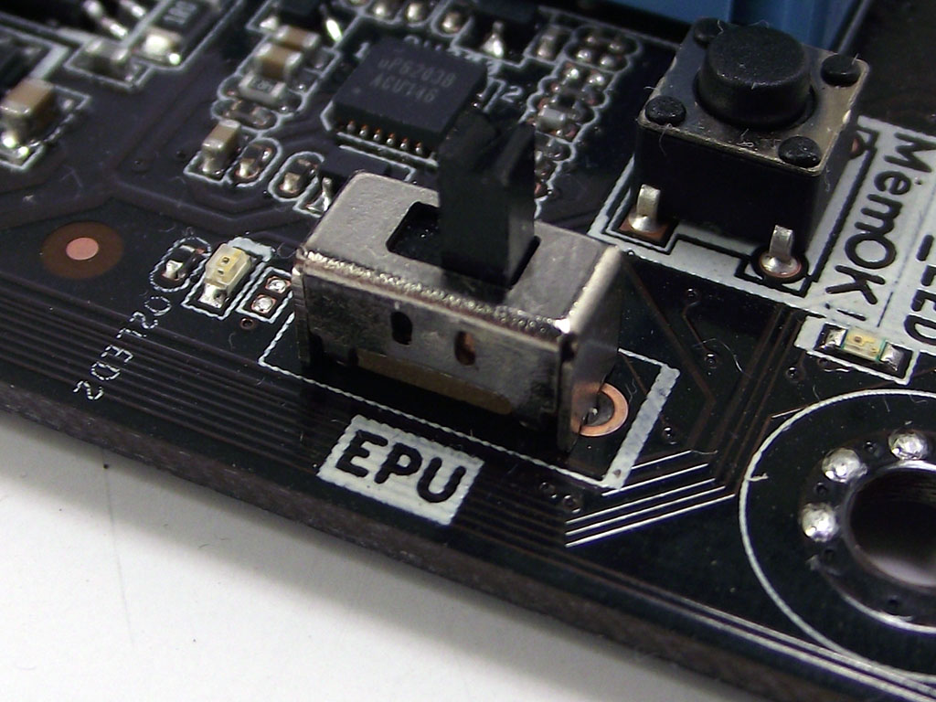
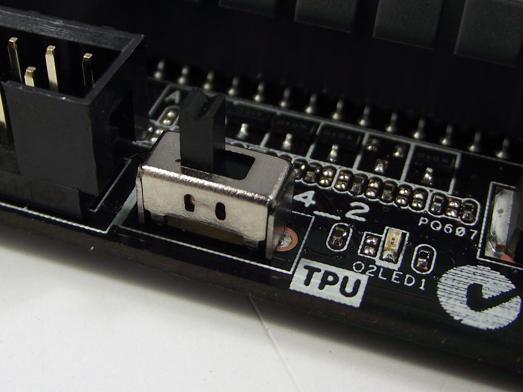
There are two onboard switches that enable automatic modes for each of the "Dual Intelligent Processors II" controllers, with the TPU switch enabling an automatic overclock safe for the majority of processors, and the EPU switch enabling automatic power savings based on load dynamics. Simply flip the switch, and on the next boot either mode will be enabled, with a nearby LED indicating when the switches are in the "ON" position.
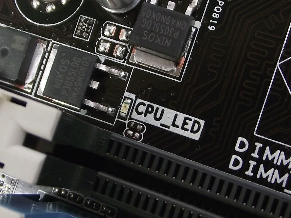
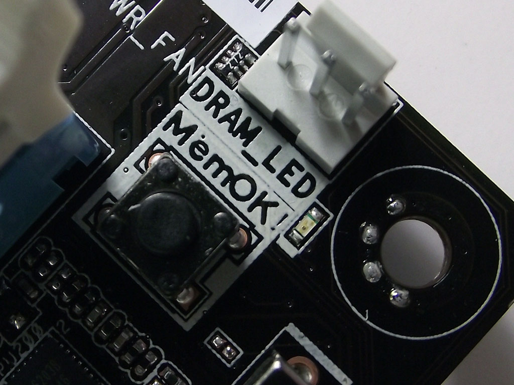

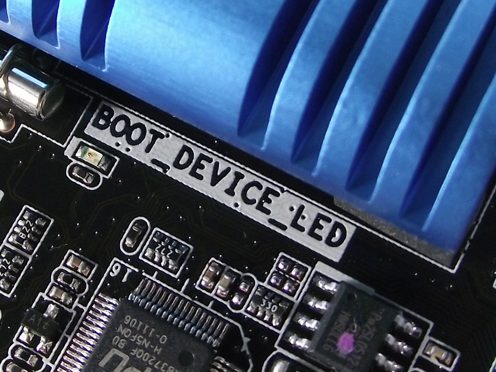
When you do boot the system, ASUS has included a POST reader of sorts, with a series of four LEDs in appropriate places that each light in succession as the board goes through the POST process. Should boot fail during any of these stages, the LED will remain lit, notifying the user of where to look for the source of the problem.

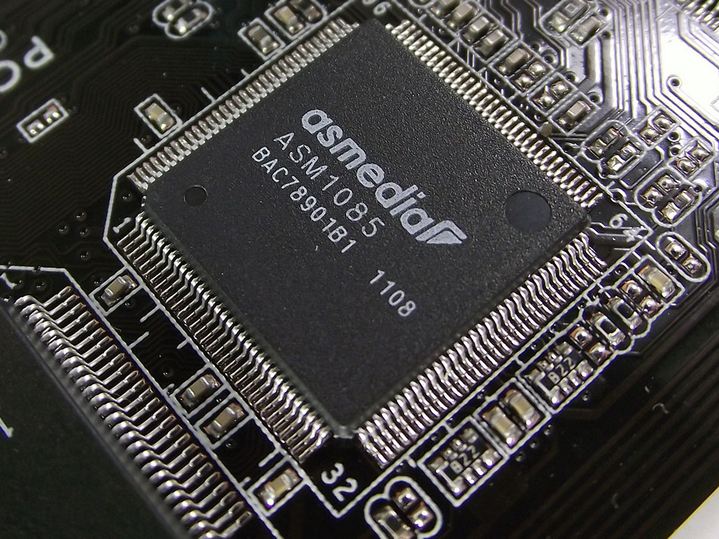
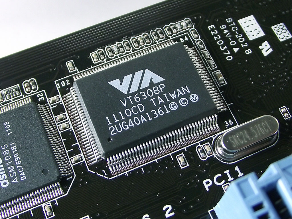
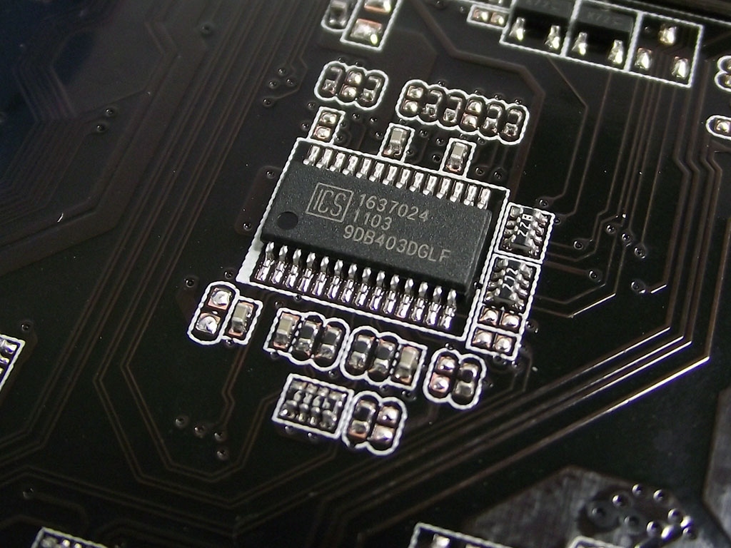
For Super I/O functionality, we find a chip we haven't seen before, the Nuvoton NCT6776F, responsible for temperature and voltage monitoring as well as fan control. The ASMedia 1085 PCIe to PCI bridge provides support for the two included PCI slots, while the VIA VT6308P drives the FireWire ports. We also find, interestingly enough, an IDT ICS9DB403 PCIe clock buffer, right above the PCIe slots.
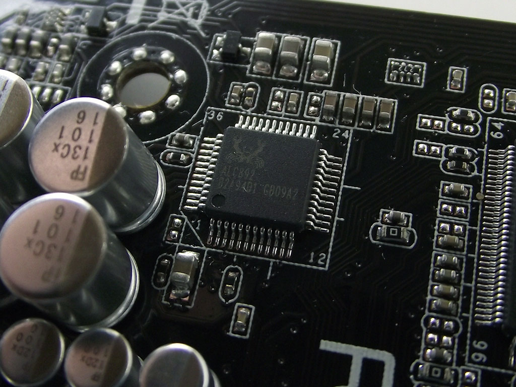
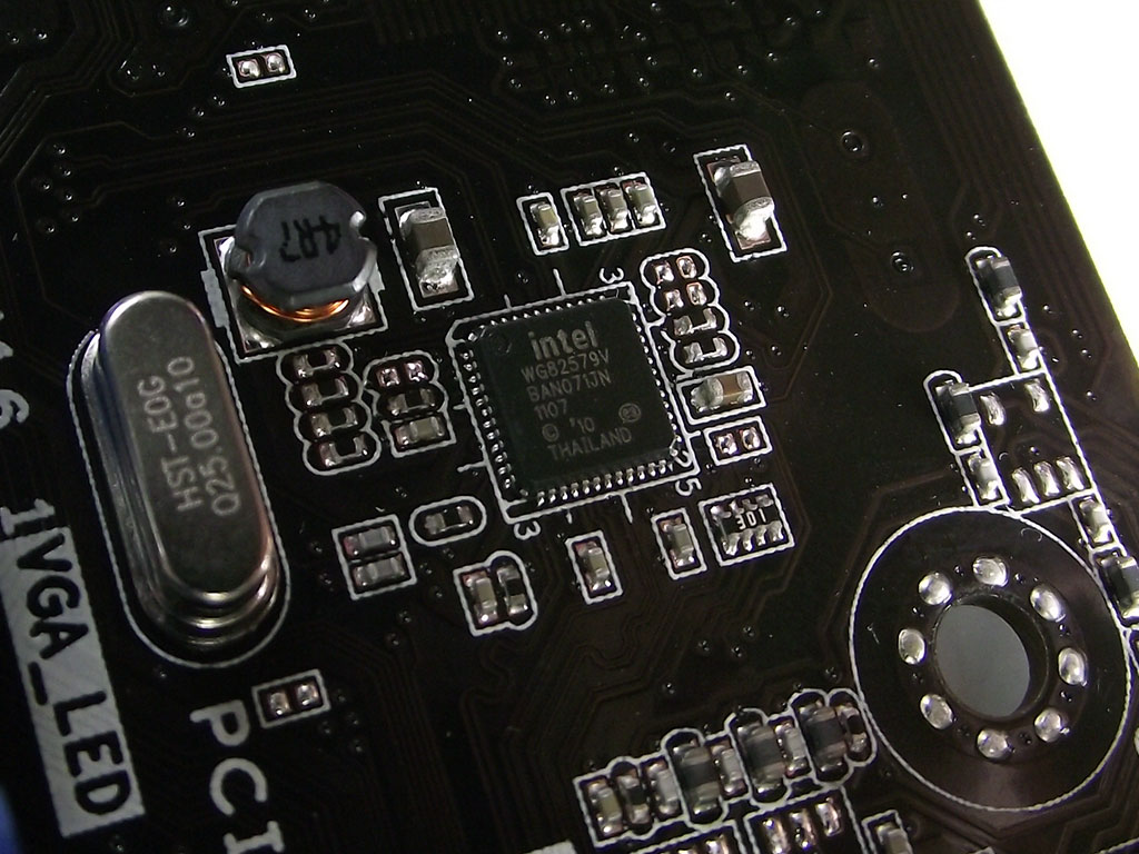
ASUS has outfitted the P8P67 PRO with audio from Realtek, none other than the ALC892, capable of HD Audio output. This newer high-end component is one of our many recent favorites, as were happy to see it here. The Intel WG82579 LAN controller is equally as impressive, yet another chip not commonly seen.

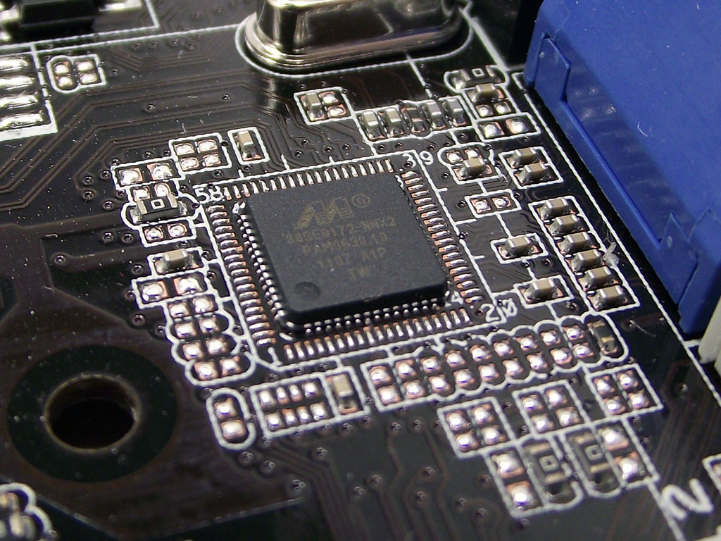
We find two identical NEC/Renesas USB3.0 controllers on the ASUS P8P67 PRO, one just above the top PCIe x1 slot, the second on the other side of the board, directly under the DIMM slots. Both are the revised chips which offer added power savings at idle not seen on the previous revision of the same chip.
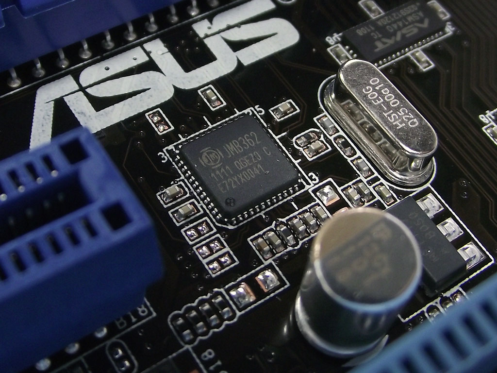
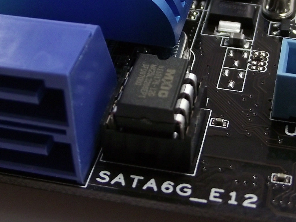
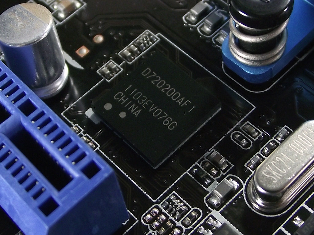
ASUS has again diverged from the norm on drive control, with a JMicron JMB362 powering the eSATA ports, while a more familiar Marvell 88SE9172 runs the dark blue internal SATA 6 Gb/s ports we mentioned earlier. The JMicron controller was a surprise, for sure, as we had hoped for eSATA 6GB/s support as well, which this specific controller does not provide.
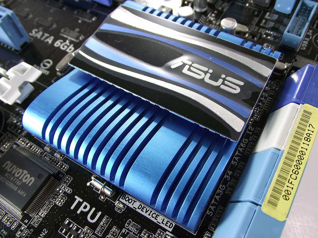

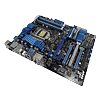
Of course, to sum up what's all on the board, we have the Southbridge and MOSFET coolers, both of which are very oversized, and well, they are almost baby blue. They remind of cool waves though, and appropriately so, given their huge size compared to what we've seen on other boards. The MOSFET heatsinks, though, did present something of what might be a problem to the obsessive like us, if you can spot it.


With the coolers removed, upon close inspection, we noticed that there was very little contact in the middle of one of the MOSFET heatsinks, and that the thermal transfer pad of the other didn't fully cover all of the MOSFETs. The Southbridge heatsink, on the other hand, was perfectly placed, which we could tell beforehand, given the amount of heat it gave off. But having read the manual's warnings to not remove the thermal solutions when certain modes are enabled, we quickly remedied the situation, and then fired the board up to begin our testing. Click the next page to get a look at the BIOS.
Apr 29th, 2024 00:27 EDT
change timezone
Latest GPU Drivers
New Forum Posts
- What's your latest tech purchase? (20372)
- Does charging protection matter? (24)
- Legion Pro 7i, i9-13900HX. PL2 limit reason in log file (2)
- Dialing in the overlock on my new 12600kf, matured silicon process showing great results... (2)
- GS110EMX switch slowing down my gigabit fiber Uploads .. Why ? what setting ? (2)
- AMD Ryzen 9 7950X3D $542 after promo (2)
- Post your Cinebench 2024 score (451)
- Your PC ATM (34525)
- Share your AIDA 64 cache and memory benchmark here (2921)
- Inconsistent cpu-z frequncies (3)
Popular Reviews
- Ugreen NASync DXP4800 Plus Review
- HYTE THICC Q60 240 mm AIO Review
- MOONDROP x Crinacle DUSK In-Ear Monitors Review - The Last 5%
- Upcoming Hardware Launches 2023 (Updated Feb 2024)
- ASUS GeForce RTX 4070 Ti Super TUF Review
- FiiO K19 Desktop DAC/Headphone Amplifier Review
- AMD Ryzen 7 5700X Review - Finally an Affordable 8-Core
- Thermalright Phantom Spirit 120 EVO Review
- NVIDIA GeForce RTX 4080 Super Founders Edition Review - Savings of $200
- Logitech G Pro X Superlight 2 Review - Updated with 4000 Hz Tested
Controversial News Posts
- Windows 11 Now Officially Adware as Microsoft Embeds Ads in the Start Menu (139)
- Sony PlayStation 5 Pro Specifications Confirmed, Console Arrives Before Holidays (117)
- NVIDIA Points Intel Raptor Lake CPU Users to Get Help from Intel Amid System Instability Issues (106)
- AMD "Strix Halo" Zen 5 Mobile Processor Pictured: Chiplet-based, Uses 256-bit LPDDR5X (103)
- US Government Wants Nuclear Plants to Offload AI Data Center Expansion (98)
- AMD's RDNA 4 GPUs Could Stick with 18 Gbps GDDR6 Memory (95)
- Windows 10 Security Updates to Cost $61 After 2025, $427 by 2028 (84)
- TechPowerUp Hiring: Reviewers Wanted for Motherboards, Laptops, Gaming Handhelds and Prebuilt Desktops (82)