 57
57
ASUS Radeon RX 5700 XT TUF EVO Review - Improved Cooler, Tested
(57 Comments) »Introduction
We have with us for review the ASUS Radeon RX 5700 XT TUF Gaming EVO. This is the fastest graphics card in the ASUS TUF Gaming family of durable yet value-positioned cards. The TUF Gaming ecosystem includes not just motherboards, graphics cards, and gaming peripherals by ASUS, but even extends to third-party memory, SSD, case, and PSU makers. This is the second TUF Gaming-branded RX 5700 XT model. The original TUF Gaming RX 5700 and RX 5700 XT cards, which launched among the first wave of Navi 10 custom designs last August, were heavily criticized by reviewers for having some of the worst thermals and noise levels. Acting on this feedback, ASUS redesigned the card with a new heatsink design, a trio of its "Axial Tech" webbed-impeller fans, and an airier cooler shroud. To differentiate this newer card from the original, ASUS added "EVO" to the model name.
The AMD Radeon RX 5700 XT is AMD's fastest graphics card based on its 7 nm "Navi" silicon that uses the RDNA architecture succeeding "Vega." The RDNA graphics architecture introduces a new generation of number-crunching machinery that brings out significant hardware changes over the "Vega" NGCU for higher performance, coupled with upgraded display and media engines that have caught up with the times. The RX 5700 XT also uses GDDR6 memory. An interesting series of price adjustments and product launches ensure that even at its starting price of $399, it offers slightly better price to performance than NVIDIA.
In this ASUS RX 5700 XT TUF EVO review, we'll definitely check on whether the current $420 price tag makes sense for the TUF, especially since you can now find some lower-end RX 5700 XT models for just $379.

At the heart of the Radeon RX 5700 XT is the 7 nm "Navi 10" silicon with an impressive 10.3 billion transistors crammed into a 251 mm² die. Unlike the "Vega 20", Navi is a more traditional GPU in that the package only has the GPU die and is surrounded by memory chips. AMD opted for cost-effective 256-bit GDDR6 memory over exotic design choices, such as HBM2. At a memory frequency of 14 Gbps, Navi enjoys a healthy memory bandwidth of 448 GB/s. It also features the latest-generation PCI-Express gen 4.0 x16 host interface with full backwards compatibility for older generations of PCIe, so you can pair it with AMD's new Ryzen 3000 processors on an X570 chipset motherboard. The buzz-words "7 nm" and "PCIe gen 4.0" are extensively used in AMD's marketing, as if to suggest that Navi is a generation ahead of NVIDIA's Turing, which is built on 12 nm and has PCIe gen 3.0. The RX 5700 XT is hence targeted at 1440p gaming with maxed out details, although compared to NVIDIA graphics chips such as the RTX 2060 Super, you lose out on ray-tracing features.
ASUS positions its TUF Gaming family a notch below its coveted ROG STRIX family of graphics cards. We in fact reviewed the RX 5700 XT ROG STRIX OC and found it to be among the strongest custom-design RX 5700 XT offerings. The RX 5700 XT TUF EVO in this review offers a beefier heatsink than the original RX 5700 XT TUF and has three Axial Tech fans that are designed to direct all of their airflow axially (onto the heatsink), with impeller webbing preventing lateral flow. ASUS also made serious efforts to lower the temperatures of the VRM and memory areas by giving them thermal pads to even the card's metal backplate. The company is said to have spent a lot of time optimizing the card's thermals and noise.
| Price | Shader Units | ROPs | Core Clock | Boost Clock | Memory Clock | GPU | Transistors | Memory | |
|---|---|---|---|---|---|---|---|---|---|
| RX 5600 XT | $270 | 2304 | 64 | 1375 MHz | 1560 MHz | 1500 MHz | Navi 10 | 10300M | 6 GB, GDDR6, 192-bit |
| RTX 2060 | $300 | 1920 | 48 | 1365 MHz | 1680 MHz | 1750 MHz | TU106 | 10800M | 6 GB, GDDR6, 192-bit |
| RX 5700 | $320 | 2304 | 64 | 1465 MHz | 1625 MHz | 1750 MHz | Navi 10 | 10300M | 8 GB, GDDR6, 256-bit |
| GTX 1080 | $500 | 2560 | 64 | 1607 MHz | 1733 MHz | 1251 MHz | GP104 | 7200M | 8 GB, GDDR5X, 256-bit |
| RTX 2060 Super | $400 | 2176 | 64 | 1470 MHz | 1650 MHz | 1750 MHz | TU106 | 10800M | 8 GB, GDDR6, 256-bit |
| RX Vega 64 | $390 | 4096 | 64 | 1247 MHz | 1546 MHz | 953 MHz | Vega 10 | 12500M | 8 GB, HBM2, 2048-bit |
| GTX 1080 Ti | $700 | 3584 | 88 | 1481 MHz | 1582 MHz | 1376 MHz | GP102 | 12000M | 11 GB, GDDR5X, 352-bit |
| RX 5700 XT | $380 | 2560 | 64 | 1605 MHz | 1755 MHz | 1750 MHz | Navi 10 | 10300M | 8 GB, GDDR6, 256-bit |
| ASUS RX 5700 XT TUF EVO Gaming | $420 | 2560 | 64 | 1650 MHz | 1905 MHz | 1750 MHz | Navi 10 | 10300M | 8 GB, GDDR6, 256-bit |
| RTX 2070 | $400 | 2304 | 64 | 1410 MHz | 1620 MHz | 1750 MHz | TU106 | 10800M | 8 GB, GDDR6, 256-bit |
| RTX 2070 Super | $500 | 2560 | 64 | 1605 MHz | 1770 MHz | 1750 MHz | TU104 | 13600M | 8 GB, GDDR6, 256-bit |
| Radeon VII | $600 | 3840 | 64 | 1802 MHz | N/A | 1000 MHz | Vega 20 | 13230M | 16 GB, HBM2, 4096-bit |
| RTX 2080 | $630 | 2944 | 64 | 1515 MHz | 1710 MHz | 1750 MHz | TU104 | 13600M | 8 GB, GDDR6, 256-bit |
| RTX 2080 Super | $700 | 3072 | 64 | 1650 MHz | 1815 MHz | 1940 MHz | TU104 | 13600M | 8 GB, GDDR6, 256-bit |
Packaging
The Card
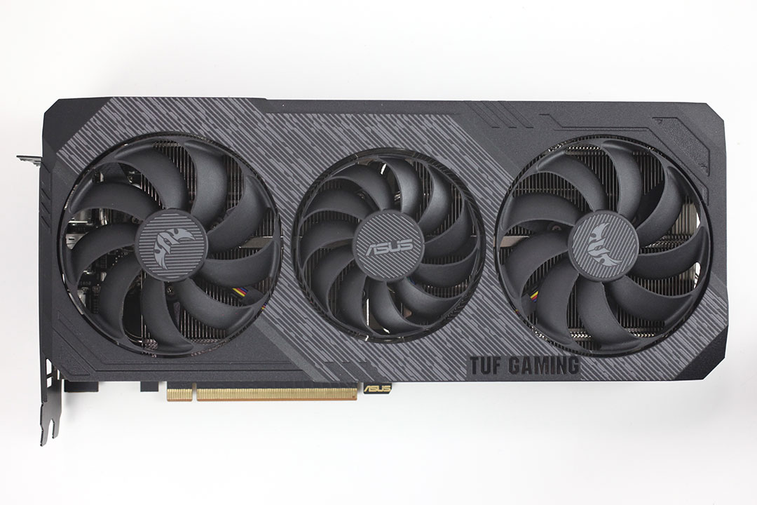


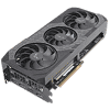
For their TUF series, ASUS created a new design identity. The card uses black and various shades of gray. Note how the center fan is smaller than the surrounding ones—this is new on the EVO version. A metal backplate in matching colors is included, too.

Dimensions of the card are 28 x 13 cm.


Installation requires three slots in your system.
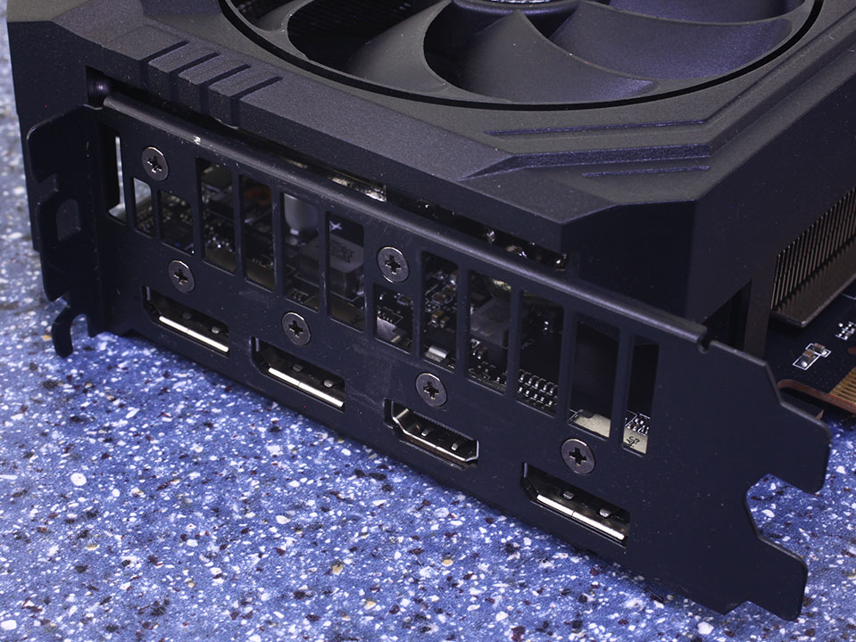
Display connectivity options include three standard DisplayPort 1.4a and an HDMI 2.0b.

The board uses one 8-pin and one 6-pin power connector. This input configuration is specified for up to 300 watts of power draw.
AMD's Navi generation of GPUs no longer supports CrossFire. DirectX 12 does include its own set of multi-GPU capabilities, but implementation requires game developers to put serious development time into a feature only a tiny fraction of their customers might ever use.
Disassembly
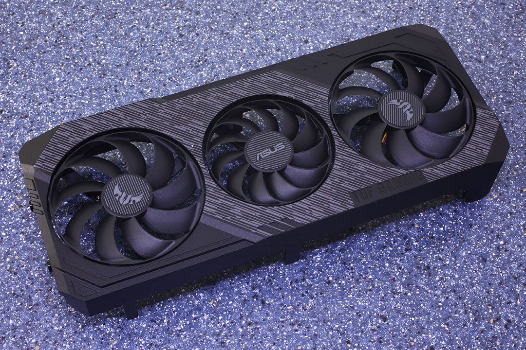
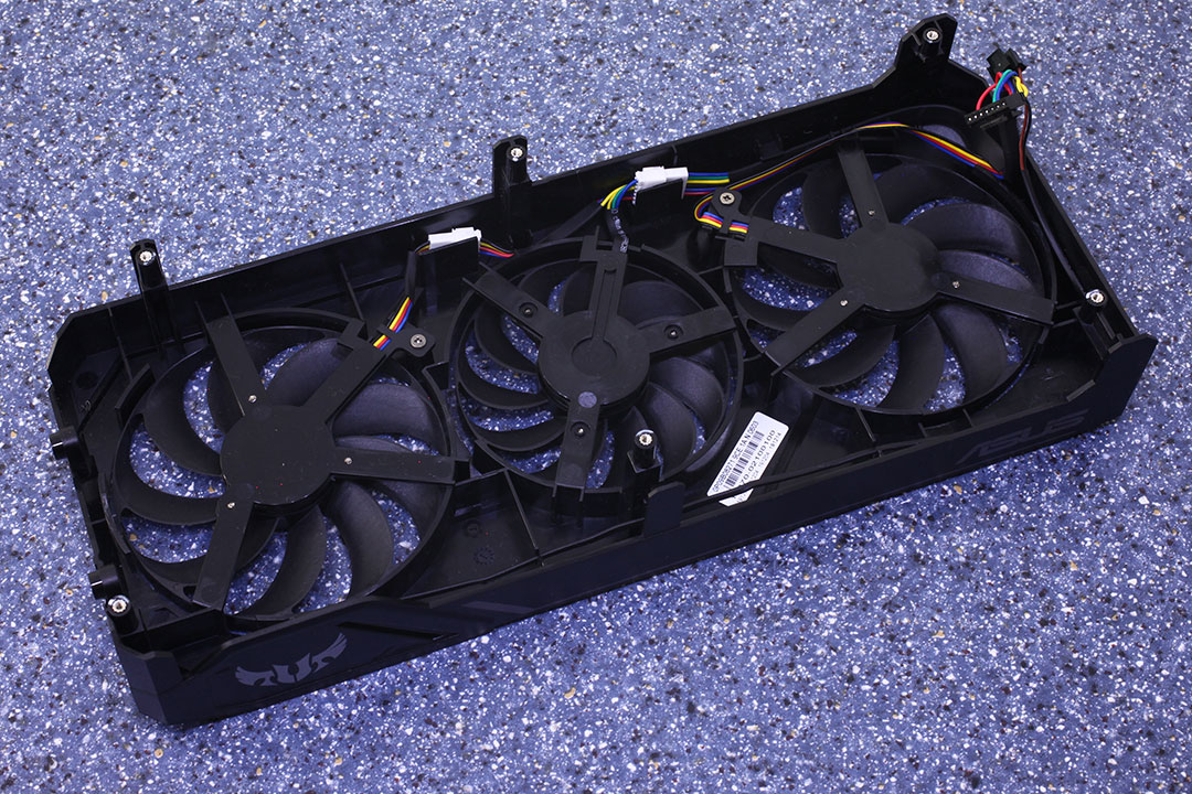
As mentioned in the introduction, ASUS had some issues with the initial batch of TUF cards, which caused public outcry from consumers and reviewers. We are testing the fixed version, which has upgraded fans with axial tech to direct the airflow through the fins. Also note how the fan impellers are surrounded by a plastic ring to ensure no air can escape horizontally. The outer fans are 90 mm in diameter, and the center fan is 80 mm across.
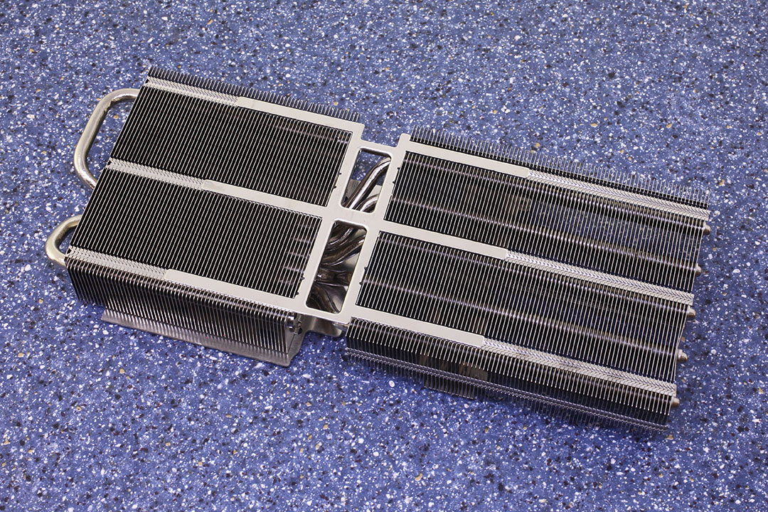

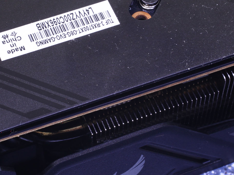
Once the cooling assembly is removed, you get access to the heatsink. It uses five heatpipes and a large array of fins to keep the card cool. This heatsink provides cooling for the GPU, memory chips, and VRM circuitry. Do note that the memory chips are cooled by a plate that is bolted to the heatsink—it is not part of it. This means that the heat transfer is slightly reduced, but still much better than on the original TUF, which just had a thin metal heatspreader on the memory that did not connect with the main heatsink at all.


The backplate is made out of metal to protect the card against damage during installation and handling. There are some thermal pads to pick up a little bit of heat from the other side of the memory chips.
High-resolution PCB Pictures
These pictures are for the convenience of volt modders and people who would like to see all the finer details on the PCB. Feel free to link back to us and use these in your articles or forum posts.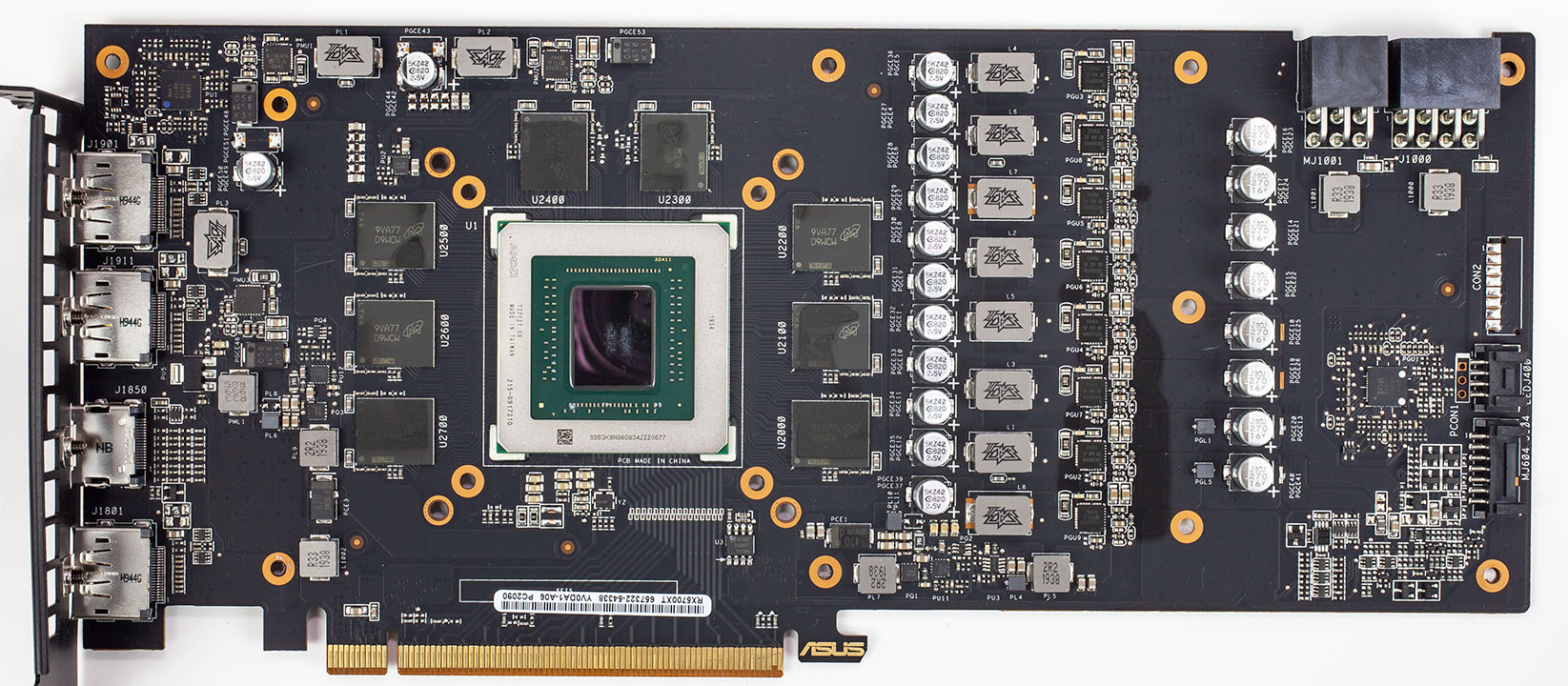
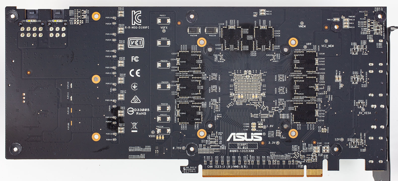
High-res versions are also available (front, back).
Circuit Board (PCB) Analysis


The GPU VRM is 7+1-phase, controlled by an International Rectifier IR35217 controller, which is among the best controllers available on the market.
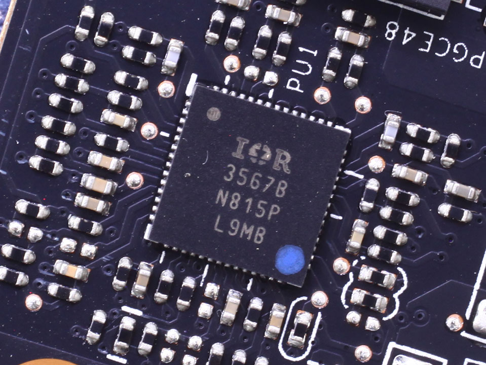

Memory voltage uses a two-phase design and is generated by an International Rectifier IR3567B controller.

The GDDR6 memory chips are made by Micron and carry the model number D9WCW, which decodes to MT61K256M32JE-14:A. They are specified to run at 1750 MHz (14 Gbps GDDR6 effective).

AMD's Navi 10 graphics processor is their first chip to use the new RDNA architecture. It is produced on a 7 nanometer process at TSMC, Taiwan and has a transistor count of 10.3 billion with a die size of 251 mm².
Our Patreon Silver Supporters can read articles in single-page format.
Apr 26th, 2024 05:44 EDT
change timezone
Latest GPU Drivers
New Forum Posts
- Best SSD for system drive (83)
- TPU's Nostalgic Hardware Club (18472)
- What are you playing? (20534)
- Last game you purchased? (258)
- Alphacool CORE 1 CPU block - bulging with danger of splitting? (22)
- What's your latest tech purchase? (20344)
- Nvidia CMP 100-210 or 100HX (GV100 GPU) (9)
- Horizontal black lines popping up on my screen? (7)
- Which new games will you be buying? (320)
- What phone you use as your daily driver? And, a discussion of them. (1484)
Popular Reviews
- HYTE THICC Q60 240 mm AIO Review
- Alienware Pro Wireless Gaming Keyboard Review
- MOONDROP x Crinacle DUSK In-Ear Monitors Review - The Last 5%
- Upcoming Hardware Launches 2023 (Updated Feb 2024)
- Thermalright Phantom Spirit 120 EVO Review
- RTX 4090 & 53 Games: Ryzen 7 5800X vs Ryzen 7 5800X3D Review
- ASUS Radeon RX 7900 GRE TUF OC Review
- NVIDIA RTX 4090: 450 W vs 600 W 12VHPWR - Is there any notable performance difference?
- RTX 4090 & 53 Games: Core i9-13900K vs Ryzen 7 5800X3D Review
- RTX 4090 & 53 Games: Core i9-13900K E-Cores Enabled vs Disabled Review
Controversial News Posts
- Windows 11 Now Officially Adware as Microsoft Embeds Ads in the Start Menu (122)
- Sony PlayStation 5 Pro Specifications Confirmed, Console Arrives Before Holidays (117)
- NVIDIA Points Intel Raptor Lake CPU Users to Get Help from Intel Amid System Instability Issues (106)
- AMD "Strix Halo" Zen 5 Mobile Processor Pictured: Chiplet-based, Uses 256-bit LPDDR5X (101)
- US Government Wants Nuclear Plants to Offload AI Data Center Expansion (98)
- AMD's RDNA 4 GPUs Could Stick with 18 Gbps GDDR6 Memory (89)
- Developers of Outpost Infinity Siege Recommend Underclocking i9-13900K and i9-14900K for Stability on Machines with RTX 4090 (85)
- Windows 10 Security Updates to Cost $61 After 2025, $427 by 2028 (84)