 46
46
ASUS Radeon RX 7600 Strix OC Review
Test Setup »High-resolution PCB Pictures
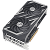
These pictures are for the convenience of volt modders and people who would like to see all the finer details on the PCB. Feel free to link back to us and use these in your articles, videos or forum posts.
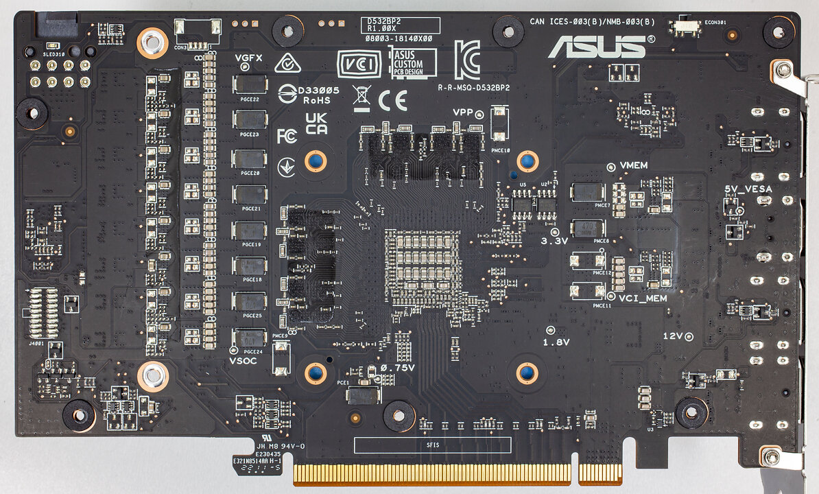
High-resolution versions are also available (front, back).
Circuit Board (PCB) Analysis
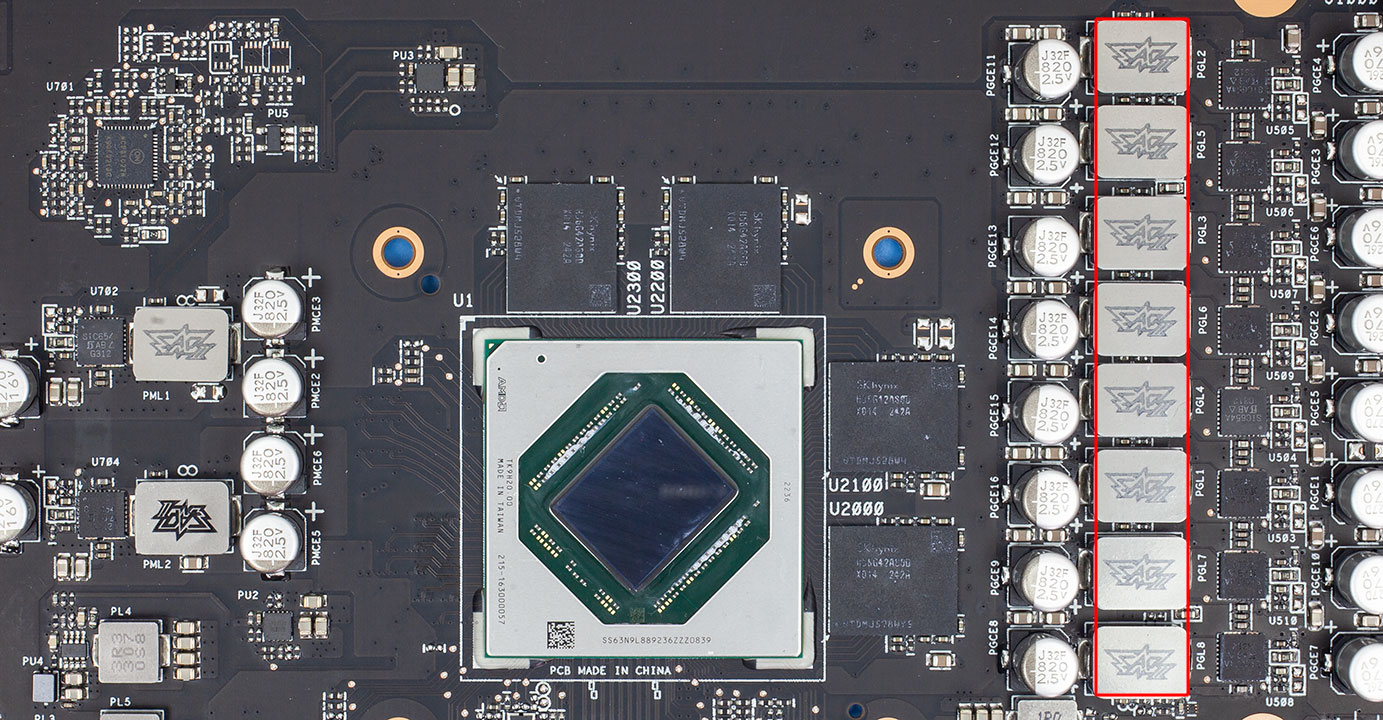

GPU VRM is an 8-phase design, driven by an International Rectifier IRF35217 controller.

The GPU VRM phases use Vishay SiC654A DrMOS, each of which is capable of 50 A current.


Memory voltage uses a two-phase design and is generated by an NCP81022N controller.

Each of the two memory phases uses the same Vishay SiC654A DrMOS as the GPU phases.

The GDDR6 memory chips are made by Hynix and carry the model number H56G42AS8DX-014. They are specified to run at 2500 MHz (20 Gbps effective).

AMD's new Navi 33 graphics processor is a monolithic design, unlike Navi 31, which powers the RX 7900 Series. It is fabricated on a 6 nm process at TSMC Taiwan with a die size of 204 mm² and 13.3 billion transistors.
Jun 16th, 2024 01:32 EDT
change timezone
Latest GPU Drivers
New Forum Posts
- when using only 2 out of 4 ram slots which 2 are best? (11)
- What are you playing? (20831)
- FINAL FANTASY XIV: Dawntrail Official Benchmark (95)
- What phone you use as your daily driver? And, a discussion of them. (1543)
- I should upgrade my gpu and psu? (16)
- Xeon Owners Club (8724)
- Opinions on AI (252)
- Is the ThermalRight Frozen Prism 360 AIO good? (103)
- Post your Speedometer 3.0 Score (47)
- ASRock Deskmini Owner's Club (34)
Popular Reviews
- Pulsar Xlite V3 eS Review
- Aune AR5000 Headphones + S17 Pro Headphones Amplifier Review
- VAXEE Outset AX Wireless (4K) Review
- Upcoming Hardware Launches 2024 (Updated May 2024)
- Team Group T-Force G70 Pro 2 TB Review
- AMD Ryzen 7 7800X3D Review - The Best Gaming CPU
- Intel Lunar Lake Technical Deep Dive - So many Revolutions in One Chip
- NZXT H6 Flow RGB Review
- ASUS Radeon RX 7900 GRE TUF OC Review
- Thermal Grizzly KryoSheet Review - Tested on RX 7900 XTX with 475 W
Controversial News Posts
- Possible Specs of NVIDIA GeForce "Blackwell" GPU Lineup Leaked (132)
- NVIDIA RTX 5090 "Blackwell" Founders Edition to Implement the "RTX 4090 Ti" Cinderblock Design (118)
- AMD Outs Ryzen 5000XT Processors for Socket AM4, an 8-year Old Socket (105)
- AMD Ryzen 9000 Zen 5 Single Thread Performance at 5.80 GHz Found 19% Over Zen 4 (105)
- Nightmare Fuel for Intel: Arm CEO Predicts Arm will Take Over 50% Windows PC Market-share by 2029 (105)
- AMD Says Ryzen 9000 Series Won't Beat 7000X3D Series at Gaming (101)
- AMD Zen 5 Storms into Gaming Desktops with Ryzen 9000 "Granite Ridge" Processors (100)
- Biden Administration to Revive Trump-Era Tariffs on China-made GPUs and Motherboards (95)