 5
5
ATI Crossfire Xpress 3200 Preview Review
(5 Comments) »Introduction
ATI, the company that is most known of their powerful and quality graphic card solutions, released their first Crossfire mainboard chipset with the RD480. Today they present the new RD580 chipset. So let's take a look what the new chipset has to offer.
Naming
Most of you already heard about "RD580" which is a sequence to RD480. The D stands for "Dual" PCI-Express video card slots. There are no plans to have an RS580 (integrated VGA) or RX580 (only one video card slot).If you talk to the chipset development team at ATI everybody just calls RD580 by the name "Skeletor". Maybe you played with Masters of the Universe "He-Man" toys as a child. Then you probably remember Skeletor as the arch-enemy of the hero He-Man. Previous chipsets had engineering names like "Metallo" and "Superman". Guess you can imagine what ATI chipset gurus were interested in when they were young.
As marketing name ATI picked "ATI Crossfire XPRESS3200". The 32 obviously stands for the 32 available graphics lanes. Sixteen lanes for every video card no matter if running with one video card or in Crossfire mode.Quick fact: ATI's chipset business made up 10% of their revenues last quarter with an expected growth to 23%
Who's XPRESS3200 for?
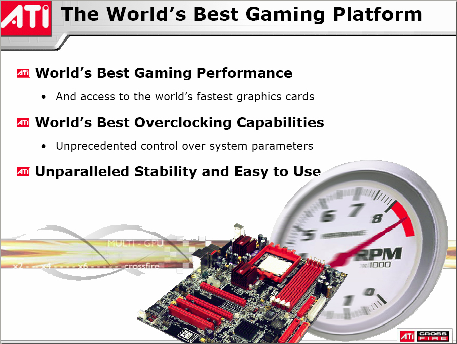
When you're taking a closer look at the picture above, you can clearly see that ATI is aiming their new chipset at extreme overclockers and hardcore gamers.
A lot of design time went into "overspeccing" the chipset. All silicon is engineered not only to work at spec but at about 30% above as well. You are basically guaranteed to overclock 30% without the need to increase voltages or cooling. ATI also had a very tight testing setup: 1.2V -5%, slow process and 120°C operating temperature. Only if the chipset was stable at these parameters it would be accepted.
Northbridge
- Smallest northbridge die in the market at 39mm² (22 million transistors)
- Manufactured on TSMC's 0.11um process node
- TDP 8 Watts

Good old saying is right here, a picture tells you more than thousand words. Size of the chipset die is very small. Smaller footprint means more chips per die, which means it is also cheaper to produce.
The reduced heat output of 7-8 Watts will greatly help integration in Media PC and Home Entertainment Systems. With such a tiny heat load you can easily get away with a small (and cheap) passive heatsink. There is no increased noise and the simple heatsink construction does not require funky cooling technologies like heatpipes to stay quiet.Quick fact: Shipped ATI chipsets in Q4/2005: Almost 7,000,000.
Our Patreon Silver Supporters can read articles in single-page format.
Apr 19th, 2024 20:46 EDT
change timezone
Latest GPU Drivers
New Forum Posts
- USB C to USB A hub (42)
- The Official Linux/Unix Desktop Screenshots Megathread (688)
- GTX 1060 6GB ASUS GPU Shuts Down after 5min of Gaming (3)
- Official Board Game Discussion (0)
- AMD RX 7000 series GPU Owners' Club (1068)
- I just succesfully baked DDR4 (69)
- I9 13890HX undervolting Suggestions (4)
- Undervolting Dell XPS 14 9440 is it possible? (7)
- Share your AIDA 64 cache and memory benchmark here (2884)
- Roccat Kone AIMO has developed a double left click, when I click it once. Any fix out there? (34)
Popular Reviews
- Horizon Forbidden West Performance Benchmark Review - 30 GPUs Tested
- Fractal Design Terra Review
- Corsair 2000D Airflow Review
- Thermalright Phantom Spirit 120 EVO Review
- Minisforum EliteMini UM780 XTX (AMD Ryzen 7 7840HS) Review
- Creative Pebble X Plus Review
- FiiO KB3 HiFi Mechanical Keyboard Review - Integrated DAC/Amp!
- ASUS GeForce RTX 4090 STRIX OC Review
- NVIDIA GeForce RTX 4090 Founders Edition Review - Impressive Performance
- ASUS GeForce RTX 4090 Matrix Platinum Review - The RTX 4090 Ti
Controversial News Posts
- Sony PlayStation 5 Pro Specifications Confirmed, Console Arrives Before Holidays (111)
- NVIDIA Points Intel Raptor Lake CPU Users to Get Help from Intel Amid System Instability Issues (102)
- US Government Wants Nuclear Plants to Offload AI Data Center Expansion (98)
- AMD "Strix Halo" Zen 5 Mobile Processor Pictured: Chiplet-based, Uses 256-bit LPDDR5X (84)
- Windows 10 Security Updates to Cost $61 After 2025, $427 by 2028 (82)
- Developers of Outpost Infinity Siege Recommend Underclocking i9-13900K and i9-14900K for Stability on Machines with RTX 4090 (82)
- TechPowerUp Hiring: Reviewers Wanted for Motherboards, Laptops, Gaming Handhelds and Prebuilt Desktops (72)
- Intel Realizes the Only Way to Save x86 is to Democratize it, Reopens x86 IP Licensing (70)