Jul 8th, 2025 14:11 CDT
change timezone
Latest GPU Drivers
New Forum Posts
- Noob question about nvme temps. (1)
- New Build (12)
- Whats Intel PCH and why its so hot? (3)
- Best motherboards for XP gaming (41)
- DTS DCH Driver for Realtek HDA [DTS:X APO4 + DTS Interactive] (2229)
- What kills gpus? (18)
- i7 2860QM how to raise power limit? (10)
- Windows 11 General Discussion (6133)
- R-T-B's PNY RTX 5080 OC Photo sideshow. (27)
- Do you still use Antivirus software on your latest hardware? (54)
Popular Reviews
- NVIDIA GeForce RTX 5050 8 GB Review
- NZXT N9 X870E Review
- Fractal Design Scape Review - Debut Done Right
- Sapphire Radeon RX 9060 XT Pulse OC 16 GB Review - An Excellent Choice
- AMD Ryzen 7 9800X3D Review - The Best Gaming Processor
- Upcoming Hardware Launches 2025 (Updated May 2025)
- Clair Obscur: Expedition 33 Performance Benchmark Review - 33 GPUs Tested
- Sapphire Radeon RX 9070 XT Nitro+ Review - Beating NVIDIA
- Corsair FRAME 5000D RS Review
- ASUS ROG Crosshair X870E Extreme Review
TPU on YouTube
Controversial News Posts
- Intel's Core Ultra 7 265K and 265KF CPUs Dip Below $250 (288)
- Some Intel Nova Lake CPUs Rumored to Challenge AMD's 3D V-Cache in Desktop Gaming (140)
- AMD Radeon RX 9070 XT Gains 9% Performance at 1440p with Latest Driver, Beats RTX 5070 Ti (116)
- NVIDIA GeForce RTX 5080 SUPER Could Feature 24 GB Memory, Increased Power Limits (115)
- NVIDIA Launches GeForce RTX 5050 for Desktops and Laptops, Starts at $249 (108)
- Microsoft Partners with AMD for Next-gen Xbox Hardware (105)
- Intel "Nova Lake‑S" Series: Seven SKUs, Up to 52 Cores and 150 W TDP (100)
- NVIDIA DLSS Transformer Cuts VRAM Usage by 20% (97)
 93
93
DDR5 CUDIMM Explained & Benched - The New Memory Standard
(93 Comments) »Introduction
The launch of DDR5 memory in 2021 came alongside Intel's 12th Generation Core processors debut and sparked mixed reactions among PC enthusiasts. Leading up to the release, many speculated that first-generation DDR5 would face challenges such as high entry costs and increased latency. This could potentially offset its benefits to gamers, leaving it less appealing than mature DDR4 offerings. This academic debate prompted TechPowerUp to publish an in-depth analysis of DDR4 and DDR5 performance with Intel's Alder Lake processor. The article findings showed at the time that DDR4 remained a strong contender, and repurposing existing DDR4 memory for a new build was still a viable option for consumers using the newest Intel processor.

In September 2022 AMD's release of the AM5 platform solidified DDR5's future market dominance, as the platform did not support DDR4. The next Intel platform (Socket 1851) and Core Ultra processors would also officially drop DDR4 support. This marked the start of a gradual sales decline of DDR4 and lower demands for the home computer consumer market. In its place, DDR5 has offered several advantages: higher operating frequencies, lower power consumption, higher density modules, and some modest system performance gains as well. Looking back at each generation of RAM, the starting and end point significantly changes over the course of the product lifespan, with both frequencies and capacity. For example, DDR4 debuted at DDR4-2133 with just 2 GB modules and evolved to up to 16 GB modules and speeds reaching DDR4-5333. Similarly, DDR5 is poised to follow this trajectory, with long-term benefits becoming more pronounced as the technology matures.
As DDR5 memory speeds continue to advance for next-generation desktops and laptops, ensuring stability and data integrity has become increasingly critical. Higher speeds bring challenges such as electronic noise and jitter, which can lead to data loss, or system instability. To address these potential issues, JEDEC, the organization responsible for memory industry standards, continue to periodically release updated DDR5 standards and requirements. In mid 2024 the JEDEC (JESD79-5C) DDR5 SDRAM standard was published, with specifications supporting up to DDR5-8800 Unbuffered DIMMs.
With memory technologies that reach mass adoption, the JEDEC organization often has a hand in the creation of their operational parameters. As such, another DRAM technology emerged in 2024 with JEDEC backing. Using a Client Clock Driver (CKD) placed on the PCB, it was designed to address clock signal loss that occurs through thermal noise, power supply noise and voltage / temperature drift. Clock signals, which are traditionally generated by the processor, are essential for maintaining synchronization across components on the motherboard and are also critical for system memory. These signals oscillate at a constant frequency between high and low states, ensuring data is transmitted and received in order. With the inclusion of a Client Clock Driver on the memory module, this addition helps "redrive" the clock signal, reducing noise and jitter while improving overall signal integrity. This is the technology we will be exploring today in this article.
CUDIMM Technology and Benefits
Covering the basics first, we start with what computer system memory is and the function. RAM, or Random Access Memory, is an essential component in computers, whether it's a laptop, desktop, servers or NUC. Each RAM module is known as a DIMM (Dual In-line Memory Module), with UDIMMs (Unbuffered Dual In-line Memory Modules) being the most common type of DDR5 RAM used in modern desktop PCs. DRAMs main function is to act as short term storage and quick retrieval of data for programs in an operational mode. In a more digestible description, DRAM acts as the go-to medium between much slower long storage solutions and the ultrafast on die processor cache capabilities. Whatever does not fit inside the processors internal cache, must be stored and accessed somewhere else. The faster this "other" storage solution is, the quicker a processor can complete its full computation. The common phase "in system memory" has only one contextual reference and means exactly what is stated. Program data is read from the slower data transfer storage mediums like Mechanical Hard Drives and Solid State Disks to System Memory while the program is running. This allows for the program data to be quick and responsive to the needs of the user as the computer processor no longer had to access the much slower data storage solutions.The downside of system memory is the volatility of data integrity. The data in question stays in distinct high and low voltages states stored inside memory banks. These banks have rows and columns for organization of data, which makes up the internals of the RAM Integrated Circuit (IC). The idea behind the JEDEC organization and standard is for the preservation of data integrity by creating operational parameters, which is used for the creation of new types of memory and future client needs.
Modern system memory started out as Synchronous Dynamic Random-Access Memory (SDRAM). Data and Commands were limited to one operation per clock cycle. With the release of DDR (Double Data Rate) Commands were still limited to one per clock cycle, but read and writes could now be performed on the raise and fall of the clock cycle. This was the starting point of the actual operating clock speed not being direct 1:1 representation of data transfer rates. A more useful term is Mega Transfers (MT). By using DDR5-4800 as example, it is effectively operating at 4800 MHz, but actually it is instead just 2400 MHz. Another way of saying this is 4800 MT/s. The ambiguous nature of DDR is that each iteration adds another layer of complexity that requires innovation to solve. DDR5 hit a roadblock in its expanse; signal integrity at higher memory speeds.
Que CUDIMM!


Client Clock Driver (CKD) is located in the middle
While DDR5 RAM is already incredibly fast and highly responsive, further advancements are needed to push its performance to even greater heights. One of the primary challenges is signal integrity, which currently limits DDR5 UDIMMs from achieving the same level of stability at the same frequency across different platforms. With the wide variety of capacity and performance orientated options available to consumers on multiple platforms, compatibility issues exponentially increase. At the core, these compatibility issues are often related to electrical challenges like single strength, noise and jitter. This is often the main contributing factor defining the max memory speed of motherboards.
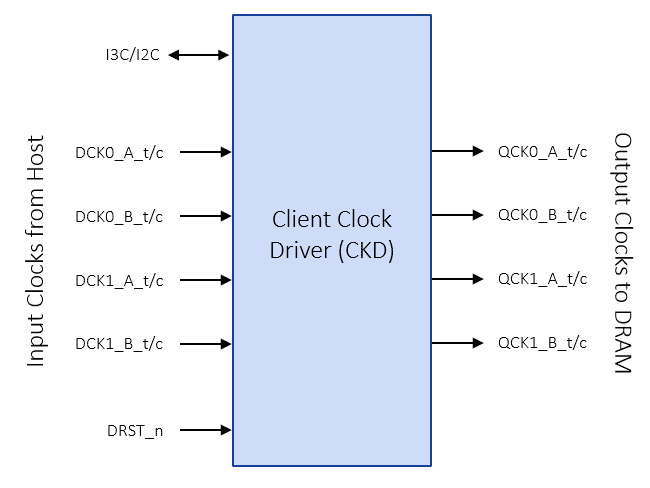
Image courtesy of RAMBUS
This problem had to be addressed to enable the next generation of faster, more reliable memory technologies. Que the Clock Driver! This is the backbone of CUDIMM, CSODIMM, and CAMM. By incorporating a clock redriver directly on the memory module, CUDIMMs enhance signal integrity, leading to improved stability and enabling higher operating frequencies. Its primary function is to buffer the clock between the host controller, ie; CPU Integrated Memory Controller (IMC) and the DRAM. To distinguish these new modules from legacy DDR5 designs without a clock driver, JEDEC introduced a naming convention that adds a "C" for "Clock" resulting in the new module types: CUDIMM (Clocked Unbuffered DIMM) and CSODIMM (Clocked Small Outline Dual Inline Memory Module). CAMM2 (Compression Attached Memory Module V2) is the outlier with the "C" not referencing a Clock Driver IC, but can be included as well. This distinction between UDIMM and CUDIMM is critical because CUDIMM and CSODIMM products are designed to use the same sockets, pins and protocols as traditional DDR5 UDIMMs and SODIMMs. Without proper motherboard support, it will operate in bypass mode by default. This gives limited backwards compatibility, but it can no longer subjected to the same operational frequency it was intended for in this bypass mode.
Our Patreon Silver Supporters can read articles in single-page format.
Jul 8th, 2025 14:11 CDT
change timezone
Latest GPU Drivers
New Forum Posts
- Noob question about nvme temps. (1)
- New Build (12)
- Whats Intel PCH and why its so hot? (3)
- Best motherboards for XP gaming (41)
- DTS DCH Driver for Realtek HDA [DTS:X APO4 + DTS Interactive] (2229)
- What kills gpus? (18)
- i7 2860QM how to raise power limit? (10)
- Windows 11 General Discussion (6133)
- R-T-B's PNY RTX 5080 OC Photo sideshow. (27)
- Do you still use Antivirus software on your latest hardware? (54)
Popular Reviews
- NVIDIA GeForce RTX 5050 8 GB Review
- NZXT N9 X870E Review
- Fractal Design Scape Review - Debut Done Right
- Sapphire Radeon RX 9060 XT Pulse OC 16 GB Review - An Excellent Choice
- AMD Ryzen 7 9800X3D Review - The Best Gaming Processor
- Upcoming Hardware Launches 2025 (Updated May 2025)
- Clair Obscur: Expedition 33 Performance Benchmark Review - 33 GPUs Tested
- Sapphire Radeon RX 9070 XT Nitro+ Review - Beating NVIDIA
- Corsair FRAME 5000D RS Review
- ASUS ROG Crosshair X870E Extreme Review
TPU on YouTube
Controversial News Posts
- Intel's Core Ultra 7 265K and 265KF CPUs Dip Below $250 (288)
- Some Intel Nova Lake CPUs Rumored to Challenge AMD's 3D V-Cache in Desktop Gaming (140)
- AMD Radeon RX 9070 XT Gains 9% Performance at 1440p with Latest Driver, Beats RTX 5070 Ti (116)
- NVIDIA GeForce RTX 5080 SUPER Could Feature 24 GB Memory, Increased Power Limits (115)
- NVIDIA Launches GeForce RTX 5050 for Desktops and Laptops, Starts at $249 (108)
- Microsoft Partners with AMD for Next-gen Xbox Hardware (105)
- Intel "Nova Lake‑S" Series: Seven SKUs, Up to 52 Cores and 150 W TDP (100)
- NVIDIA DLSS Transformer Cuts VRAM Usage by 20% (97)