 75
75
EVGA GeForce RTX 3060 XC Review
Test Setup »High-resolution PCB Pictures
These pictures are for the convenience of volt modders and people who would like to see all the finer details on the PCB. Feel free to link back to us and use these in your articles or forum posts.
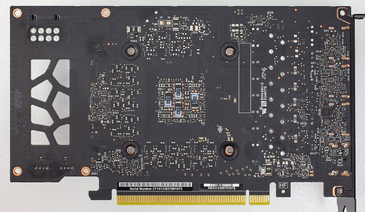
High-res versions are also available (front, back).
Circuit Board (PCB) Analysis
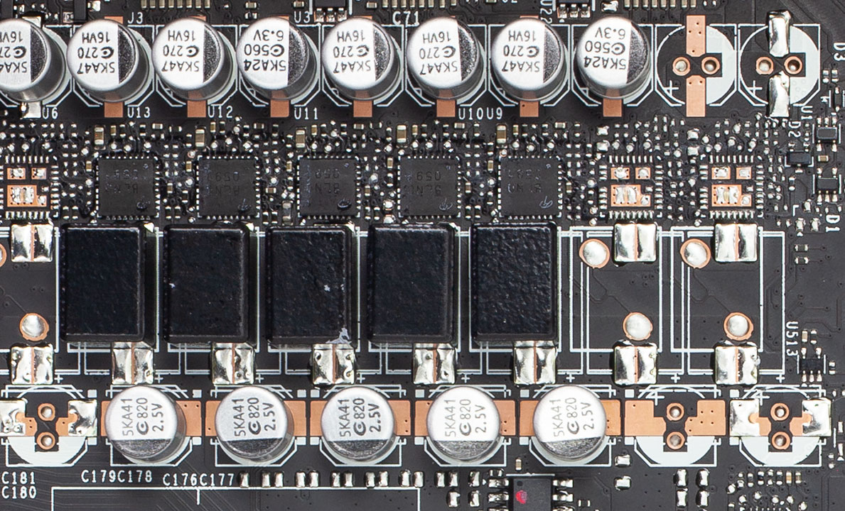
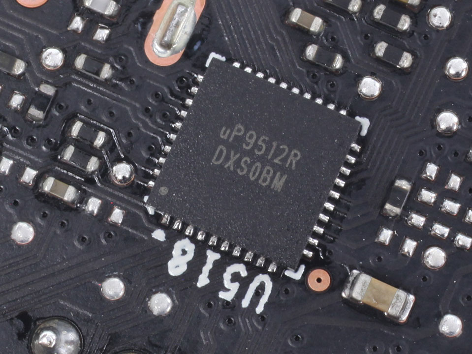
GPU voltage is 5-phase and managed by an uPI uP9512R controller.
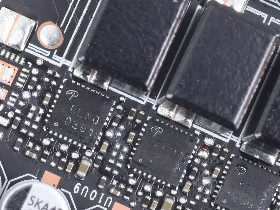
The DrMOS chips for the GPU are made by Alpha and Omega Semiconductor.


Memory voltage is a two-phase design generated by a uPI uP1666Q buck controller.
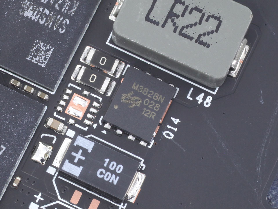
For memory, M3828N MOSFETs are used.
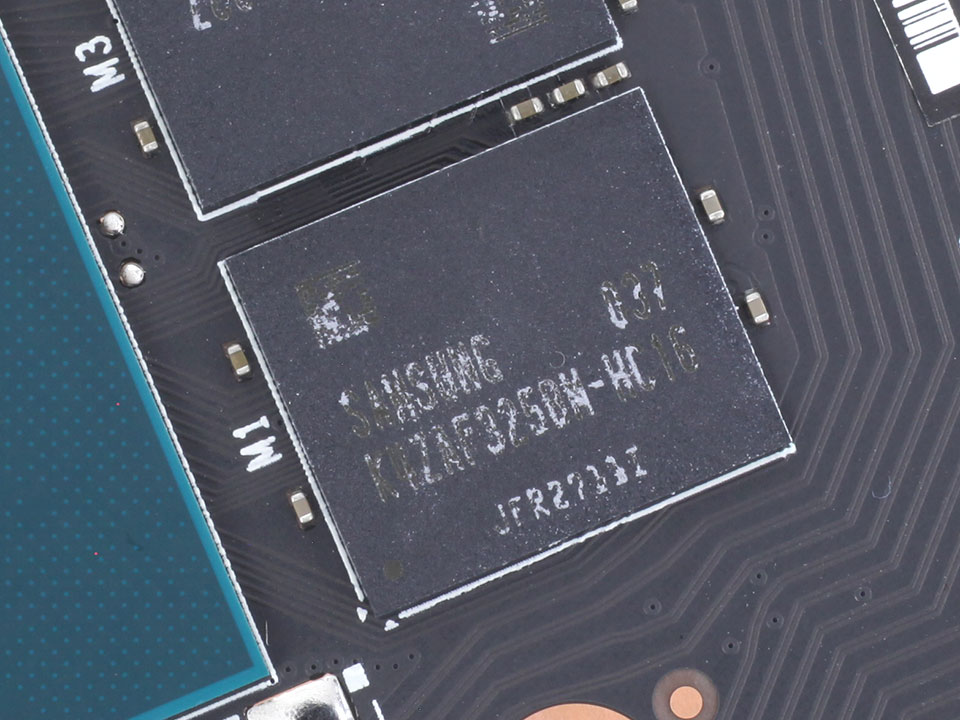
The GDDR6 chips are made by Samsung, carry the model number "K4ZAF325BM-HC16," and are rated to run at 16 Gbps.

NVIDIA's GA106 graphics processor is the company's third GeForce Ampere architecture chip. It is produced on a 8 nanometer process at Samsung and has a transistor count of 13.3 billion with a die size of 276 mm².
Apr 27th, 2024 04:14 EDT
change timezone
Latest GPU Drivers
New Forum Posts
- wireless mic for pc (0)
- Ryzen Owners Zen Garden (7245)
- My mouse randomly stops working (2)
- Horizontal black lines popping up on my screen? (14)
- Should I install Windows 10 or 11 for my new device (4)
- MSI Stealth GS65 9SF settings after repaste (0)
- Which terminal emulator do you use the most? (10)
- Browser startup performance test (4)
- The TPU UK Clubhouse (24789)
- List of NPU-optimized apps and games (0)
Popular Reviews
- Ugreen NASync DXP4800 Plus Review
- HYTE THICC Q60 240 mm AIO Review
- MOONDROP x Crinacle DUSK In-Ear Monitors Review - The Last 5%
- Upcoming Hardware Launches 2023 (Updated Feb 2024)
- Thermalright Phantom Spirit 120 EVO Review
- FiiO K19 Desktop DAC/Headphone Amplifier Review
- Quick Look: MOONDROP CHU 2 Budget In-Ear Monitors
- AMD Ryzen 7 7800X3D Review - The Best Gaming CPU
- Alienware Pro Wireless Gaming Keyboard Review
- Corsair iCUE Link XC7 RGB Elite CPU Water Block Review
Controversial News Posts
- Windows 11 Now Officially Adware as Microsoft Embeds Ads in the Start Menu (137)
- Sony PlayStation 5 Pro Specifications Confirmed, Console Arrives Before Holidays (117)
- NVIDIA Points Intel Raptor Lake CPU Users to Get Help from Intel Amid System Instability Issues (106)
- AMD "Strix Halo" Zen 5 Mobile Processor Pictured: Chiplet-based, Uses 256-bit LPDDR5X (103)
- US Government Wants Nuclear Plants to Offload AI Data Center Expansion (98)
- AMD's RDNA 4 GPUs Could Stick with 18 Gbps GDDR6 Memory (95)
- Developers of Outpost Infinity Siege Recommend Underclocking i9-13900K and i9-14900K for Stability on Machines with RTX 4090 (85)
- Windows 10 Security Updates to Cost $61 After 2025, $427 by 2028 (84)