 52
52
EVGA GeForce RTX 3080 FTW3 Ultra Review
Test Setup »High-resolution PCB Pictures
These pictures are for the convenience of volt modders and people who would like to see all the finer details on the PCB. Feel free to link back to us and use these in your articles or forum posts.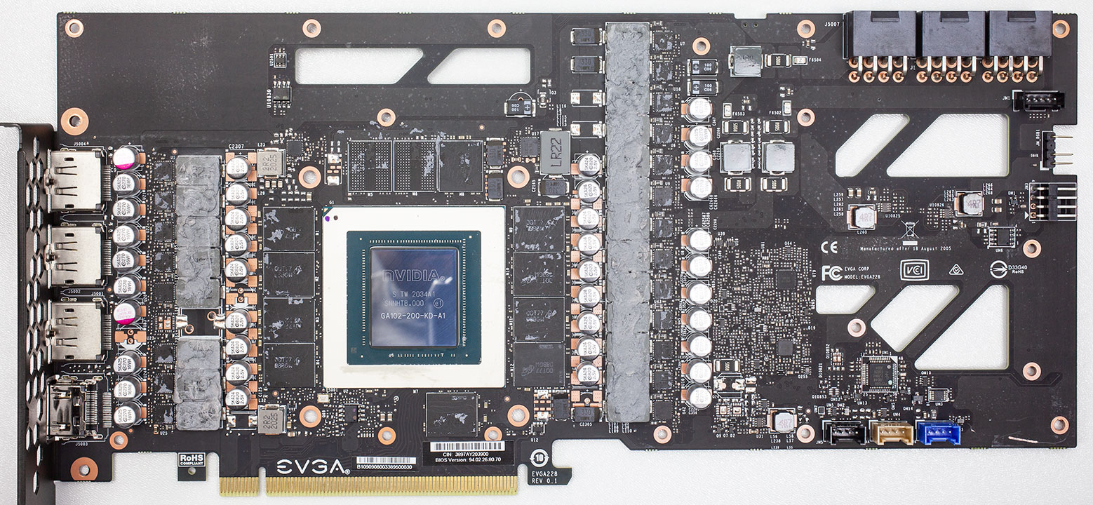
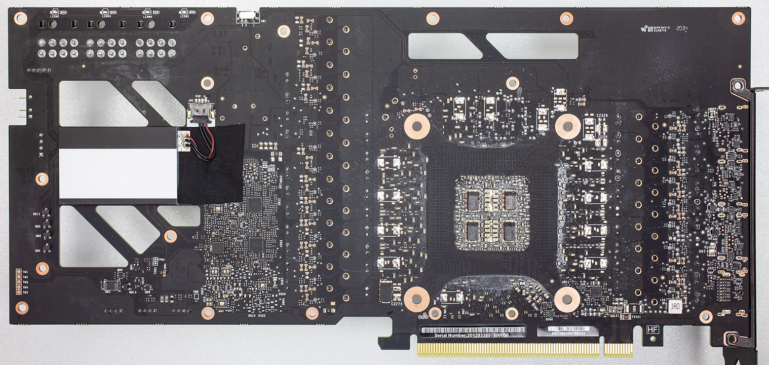
High-res versions are also available (front, back).
Circuit Board (PCB) Analysis

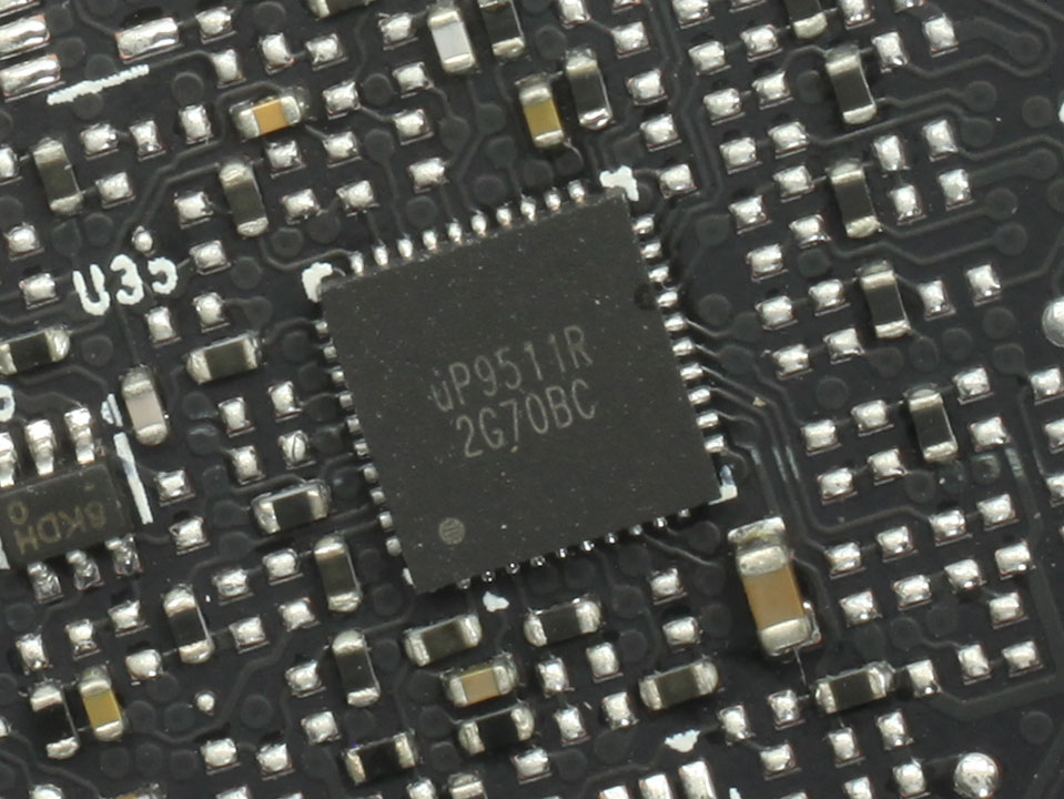
Unlike NVIDIA's Founders Edition boards, which implement MPS controllers, EVGA uses a pair of UPI 9511R controllers to manage the GPU voltage.

GPU voltage uses 19 power phases.
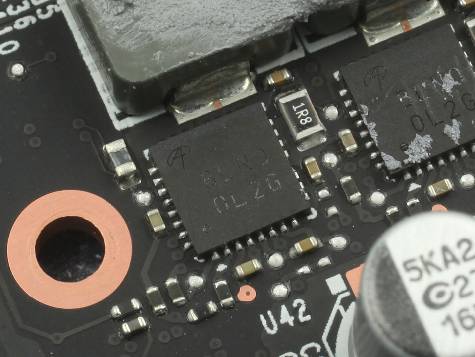
EVGA is using DrMOS components throughout the VRM.


Memory voltage uses a three-phase design and is generated by another UPI 9511R.

The GDDR6X memory chips are made by Micron and carry the model number D8BGW, which decodes to MT61K256M32JE-19:T. They are specified to run at 1188 MHz (19 Gbps GDDR6X effective).
GDDR6X doubles the data rate once again over GDDR6. It no longer transmits one bit of information by setting the voltage to either "on" or "off", but instead sends two bits of information at the same time by using four different voltage levels.

NVIDIA's GA102 graphics processor is the company's second Ampere architecture chip, the first one targeted at GeForce gamers. It is produced on a 8 nanometer process at Samsung and has a transistor count of 28 billion with a die size of 628 mm².
Apr 25th, 2024 22:15 EDT
change timezone
Latest GPU Drivers
New Forum Posts
- What are you playing? (20530)
- Secure boot already open help (0)
- TPU's Nostalgic Hardware Club (18465)
- Post your Speedometer 3.0 Score (36)
- Size on Disk Excessively Different than Size (9)
- Dell Workstation Owners Club (3056)
- Core PL1 + GPU PL1 + Ring EDP OTHER (10)
- Best SSD for system drive (80)
- Which new games will you be buying? (315)
- BSOD if I touch the pcache offset voltage in throttlestop (i9-13900hx lenovo pro 7i) (23)
Popular Reviews
- Fractal Design Terra Review
- Thermalright Phantom Spirit 120 EVO Review
- Corsair 2000D Airflow Review
- ASUS GeForce RTX 4090 STRIX OC Review
- NVIDIA GeForce RTX 4090 Founders Edition Review - Impressive Performance
- ASUS GeForce RTX 4090 Matrix Platinum Review - The RTX 4090 Ti
- MSI GeForce RTX 4090 Suprim X Review
- Gigabyte GeForce RTX 4090 Gaming OC Review
- MSI GeForce RTX 4090 Gaming X Trio Review
- MSI GeForce RTX 4090 Suprim Liquid X Review
Controversial News Posts
- Sony PlayStation 5 Pro Specifications Confirmed, Console Arrives Before Holidays (117)
- Windows 11 Now Officially Adware as Microsoft Embeds Ads in the Start Menu (108)
- NVIDIA Points Intel Raptor Lake CPU Users to Get Help from Intel Amid System Instability Issues (106)
- AMD "Strix Halo" Zen 5 Mobile Processor Pictured: Chiplet-based, Uses 256-bit LPDDR5X (101)
- US Government Wants Nuclear Plants to Offload AI Data Center Expansion (98)
- AMD's RDNA 4 GPUs Could Stick with 18 Gbps GDDR6 Memory (88)
- Developers of Outpost Infinity Siege Recommend Underclocking i9-13900K and i9-14900K for Stability on Machines with RTX 4090 (85)
- Windows 10 Security Updates to Cost $61 After 2025, $427 by 2028 (84)