 26
26
EVGA GTX 1070 Ti FTW2 iCX 8 GB Review
Circuit Board Analysis »A Closer Look
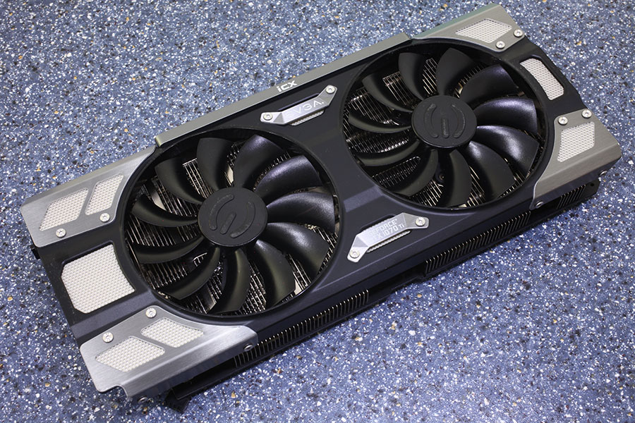
EVGA is using a cooler with five heatpipes. The bottom of the thermal assembly also provides cooling for the memory chips and VRM circuitry.


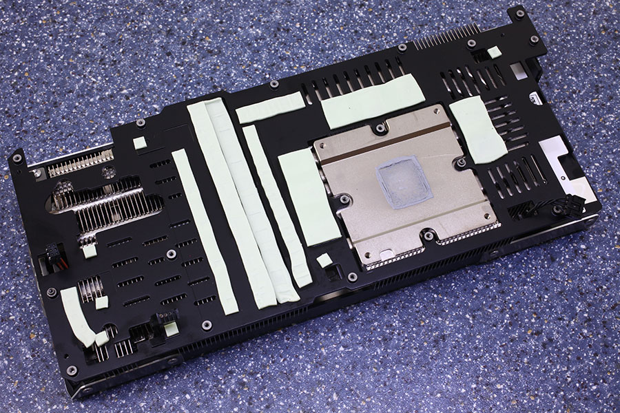
The backplate consists of two pieces, just like on the NVIDIA reference design. EVGA's idea here is to keep heat from the VRM and GPU circuitries separated. Note the thermal pads here which provide a little bit of extra cooling for either circuitry.

A BIOS switch that lets you toggle to a second BIOS with a slightly higher power-adjustment maximum has also been added (the default power limit is 180 W for either BIOS). Both BIOSes are identical otherwise.

EVGA has upgraded the power input of their card to 2x 8-pin, which is specified for up to 375 W of power input. This seems a bit overkill given the card's power consumption tops out at 210 W at stock and the board power limit after adjustments is set to 217 W on the primary BIOS and 235 W on the secondary BIOS.

With Pascal, NVIDIA made some changes to how SLI works. In a nutshell, for 4K at 60 Hz and above, NVIDIA recommends new high-bandwidth SLI bridges it dubbed "SLI HB." These bridges occupy both SLI fingers. Traditional triple- and quad-SLI setups are gone as well. Only certain benchmarks can run more than the dual-SLI setup to which all games are limited.
May 10th, 2024 09:21 EDT
change timezone
Latest GPU Drivers
New Forum Posts
- Issues with my gaming laptop (1)
- Homeworld 3 [Official Thread] (5)
- Noisy rx 6600 xt (11)
- What's your latest tech purchase? (20500)
- My Laptop is having issues with PL2 and EDP OTHER (13)
- Looking for recommendations to upgrade my ap201 (20)
- What are you playing? (20611)
- RM750x (2021) enough for my 5800X3D + 7900XT system? (15)
- RTX 4070 vs RTX 4070 Ti power scaling (10)
- Graphics card running at 8x 4.0 not 16x 4.0 (21)
Popular Reviews
- CHERRY XTRFY M64 Pro Review
- Bykski CPU-XPR-C-I CPU Water Block Review - Amazing Value!
- Corsair iCUE Link RX120 RGB 120 mm Fan Review
- Corsair MP700 Pro SE 4 TB Review
- ThundeRobot ML903 NearLink Review
- Upcoming Hardware Launches 2023 (Updated Feb 2024)
- Finalmouse UltralightX Review
- AMD Ryzen 7 7800X3D Review - The Best Gaming CPU
- Sapphire Radeon RX 7700 XT Pure Review
- ASUS Radeon RX 7900 GRE TUF OC Review
Controversial News Posts
- Intel Statement on Stability Issues: "Motherboard Makers to Blame" (264)
- AMD to Redesign Ray Tracing Hardware on RDNA 4 (206)
- Windows 11 Now Officially Adware as Microsoft Embeds Ads in the Start Menu (170)
- NVIDIA to Only Launch the Flagship GeForce RTX 5090 in 2024, Rest of the Series in 2025 (144)
- Sony PlayStation 5 Pro Specifications Confirmed, Console Arrives Before Holidays (119)
- AMD's RDNA 4 GPUs Could Stick with 18 Gbps GDDR6 Memory (114)
- NVIDIA Points Intel Raptor Lake CPU Users to Get Help from Intel Amid System Instability Issues (106)
- AMD Ryzen 9 7900X3D Now at a Mouth-watering $329 (104)