 14
FSP MEGA GM 1000 W Review
Test Methodology »Internals
We have been advised by FSP that this is a pre-production test sample, and that the internal assembly quality may not reflect that of the final production units.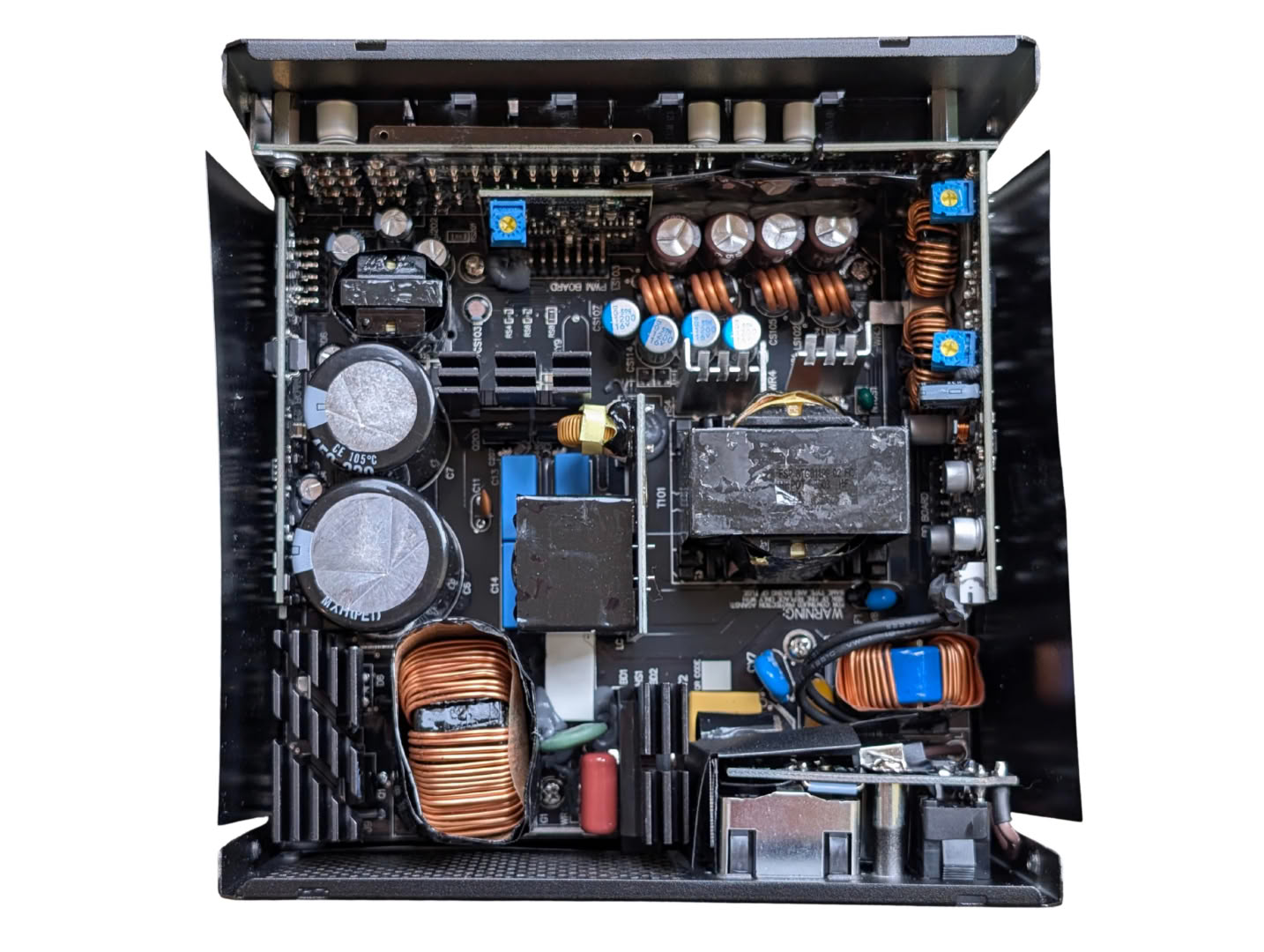
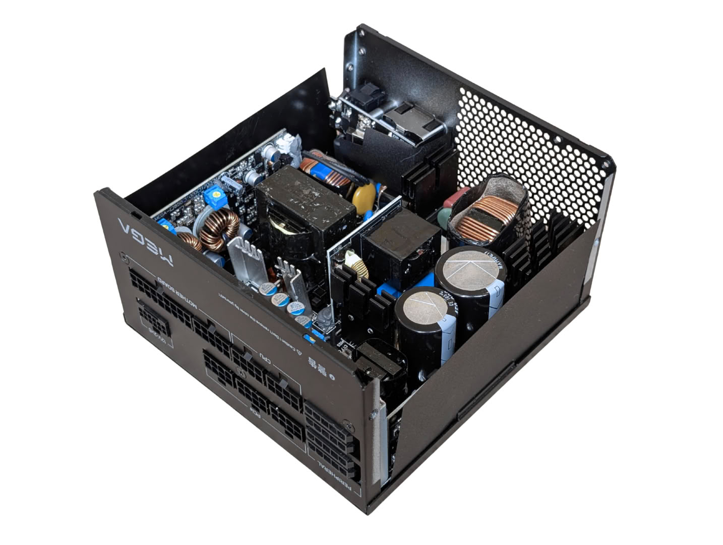
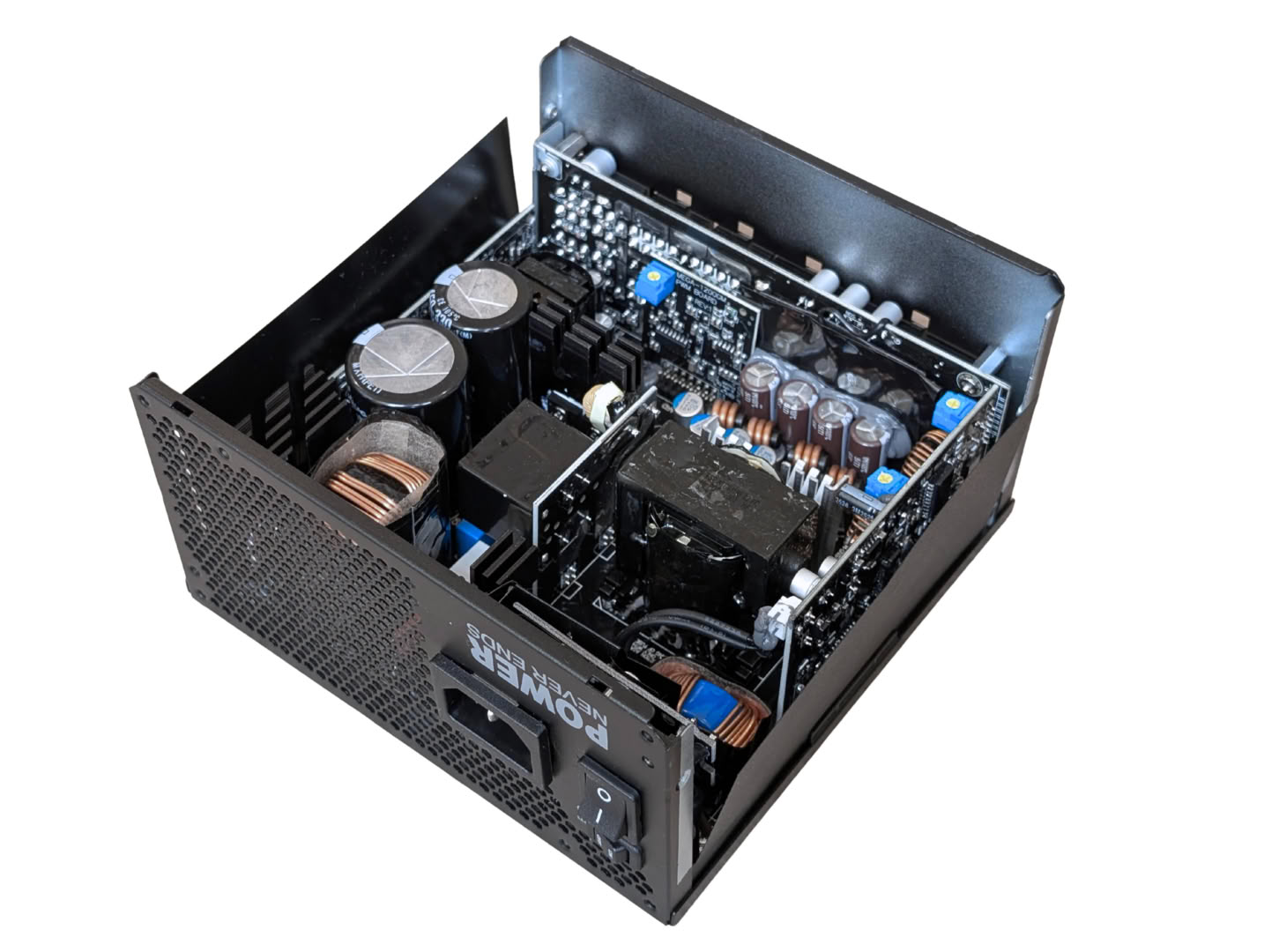
The internals follow a fairly generic layout, and it's quite easy to follow the circuit path. The components are packed in quite tightly in order to retain the 150 mm length.
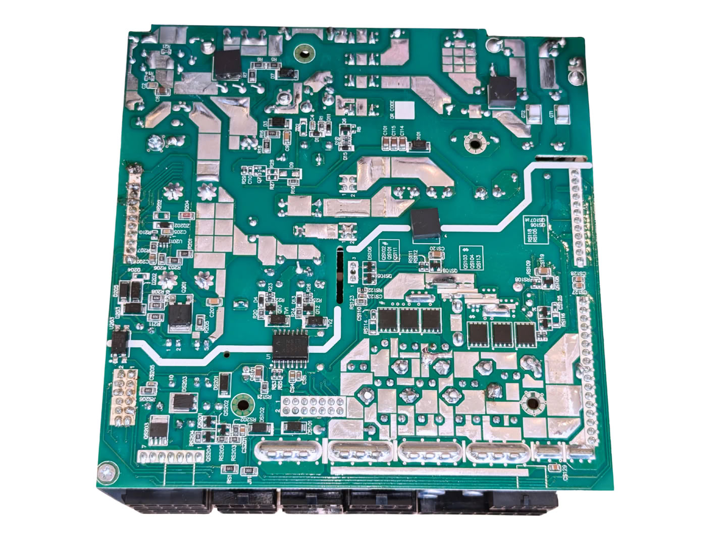
The underside of the board is also populated with SMD components including the main 12 V rail MOSFETs.
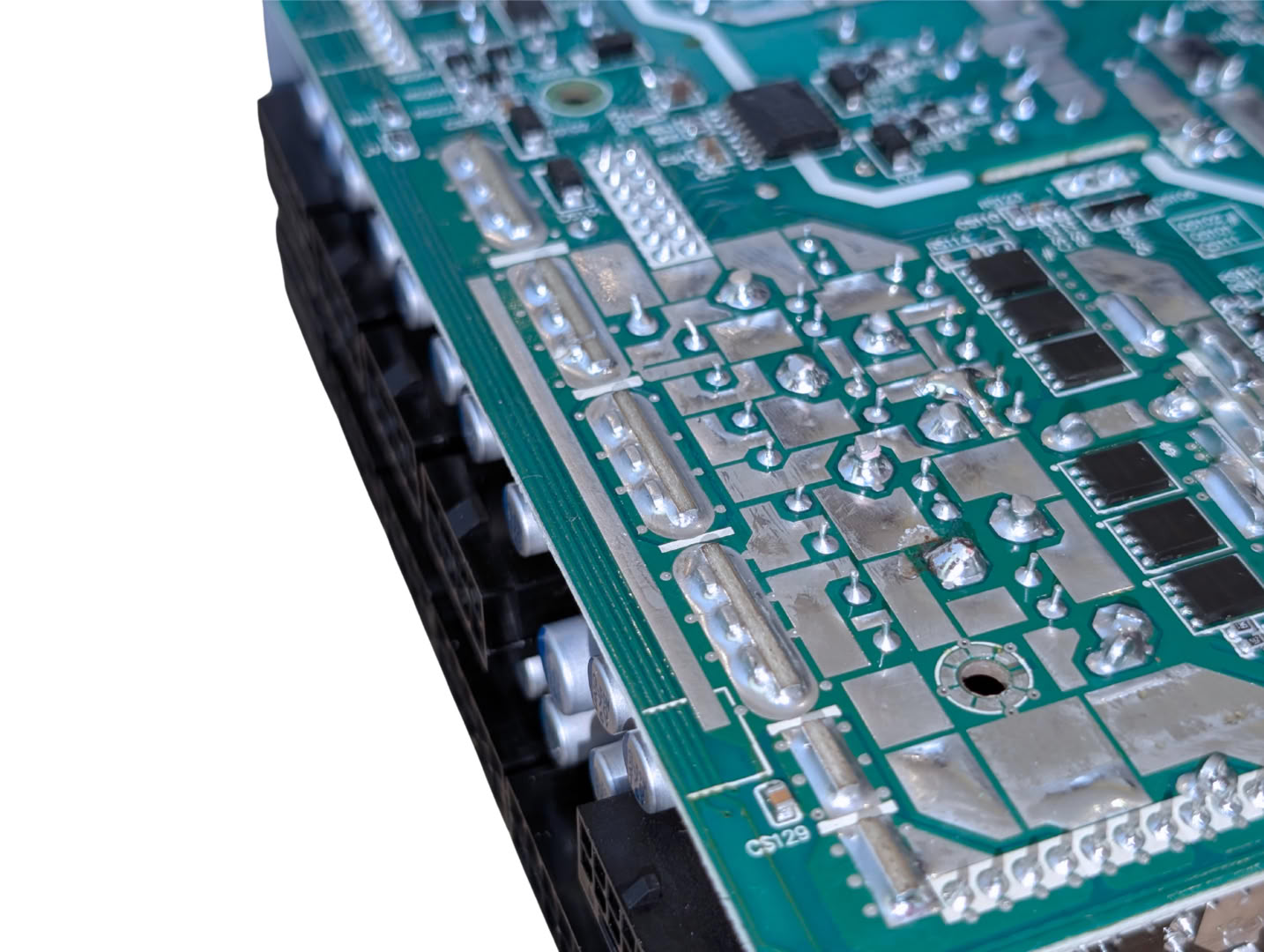
The output connector board is soldered directly to the main board at a 90-degree angle, rather than separately and attached with wires, as seen in some other power supplies.
The assembly and soldering quality has some room for improvement, especially for a flagship line.
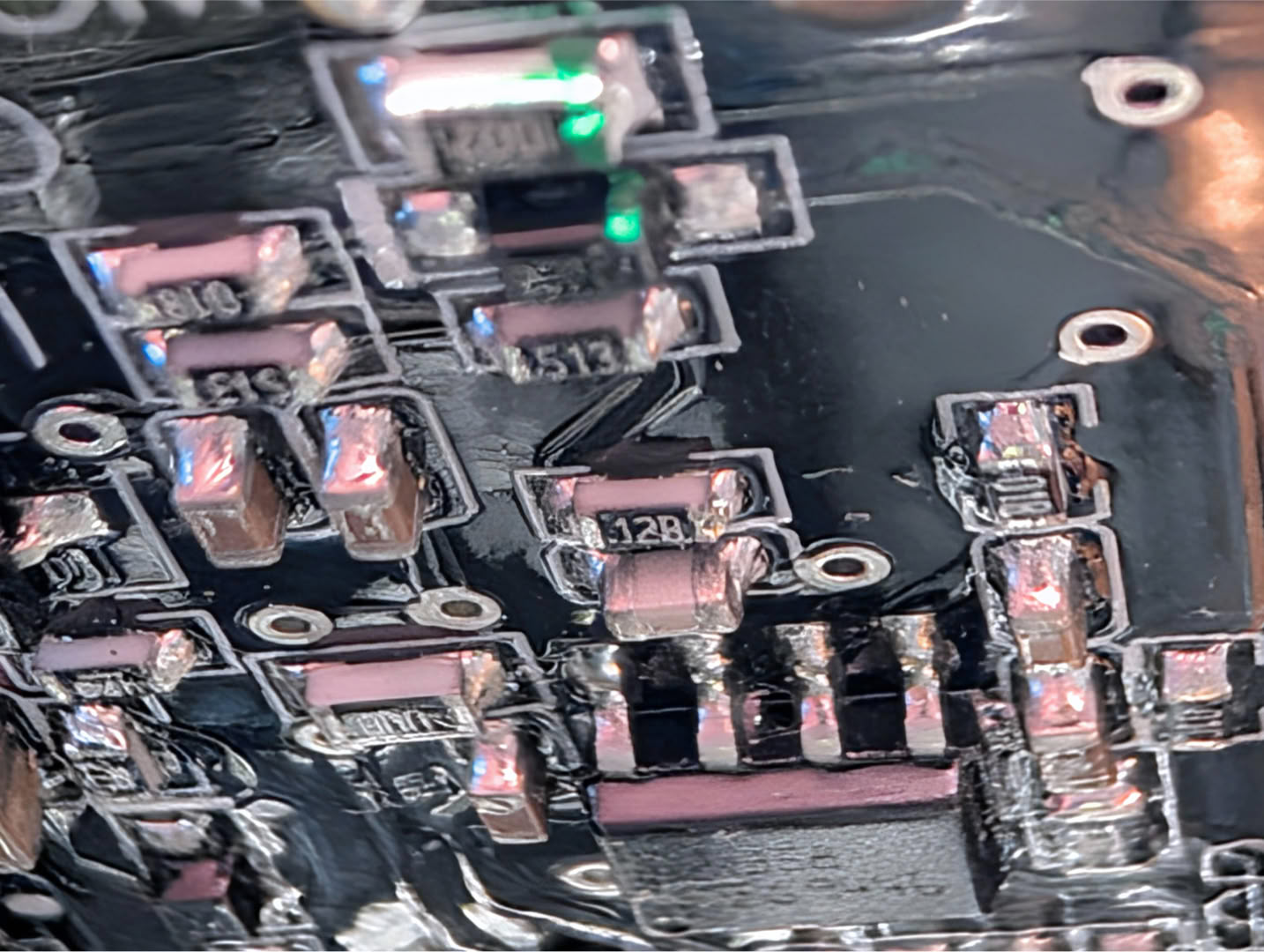
The SMD soldering is inconsistent, some resistors and components are not completely flat to the board. The solder itself doesn't seem to have flowed uniformly, and some components only have a small crumbly looking connection from their tab to the pad. With heat/cool cycles and vibrations, these can develop hairline cracks, leading to faults, instability or total failure.
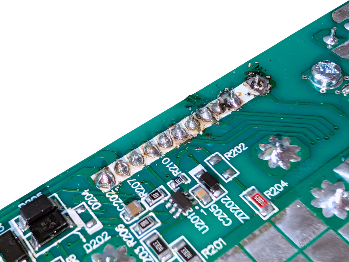
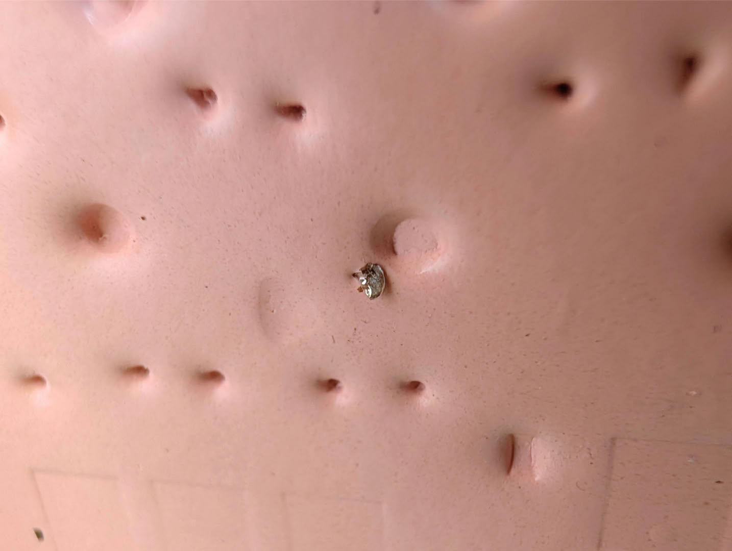
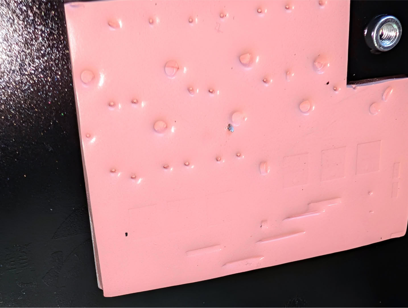
There is leftover flux and debris from hand-soldered sections, and even a ball of solder stuck to the thermal pad for the main 12 V MOSFETs. This could spell disaster if left floating around freely inside, risking not only damage to the supply, but any sensitive PC components connected to it.
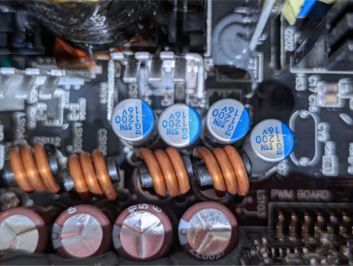
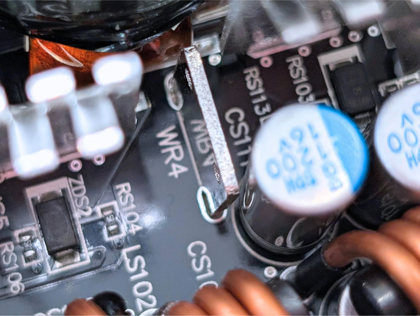
Some components have been mounted touching or very nearly touching others, for example the 12 V output filter inductors touching some capacitors. This is not initially an issue as both are insulated, but over time with vibration and heat, the insulation can eventually rub through and short out these components. It's not a risk worth taking.
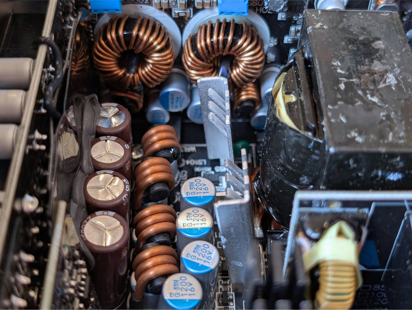
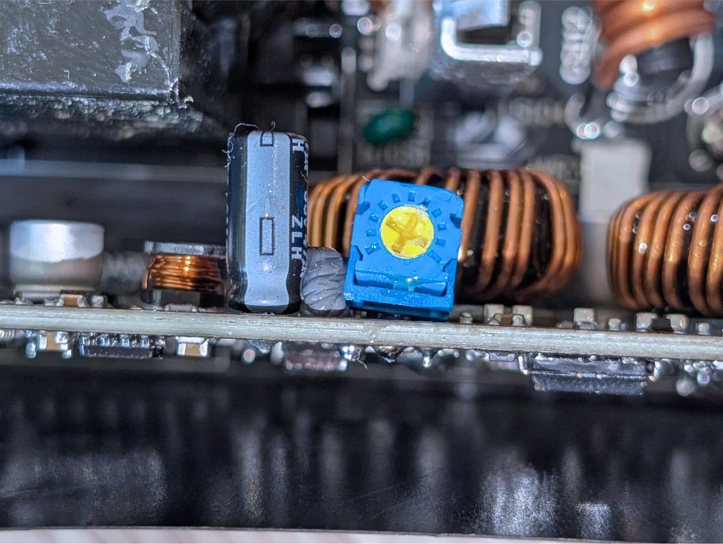
The component placement is overall a bit untidy, although this alone doesn't affect operation or performance.
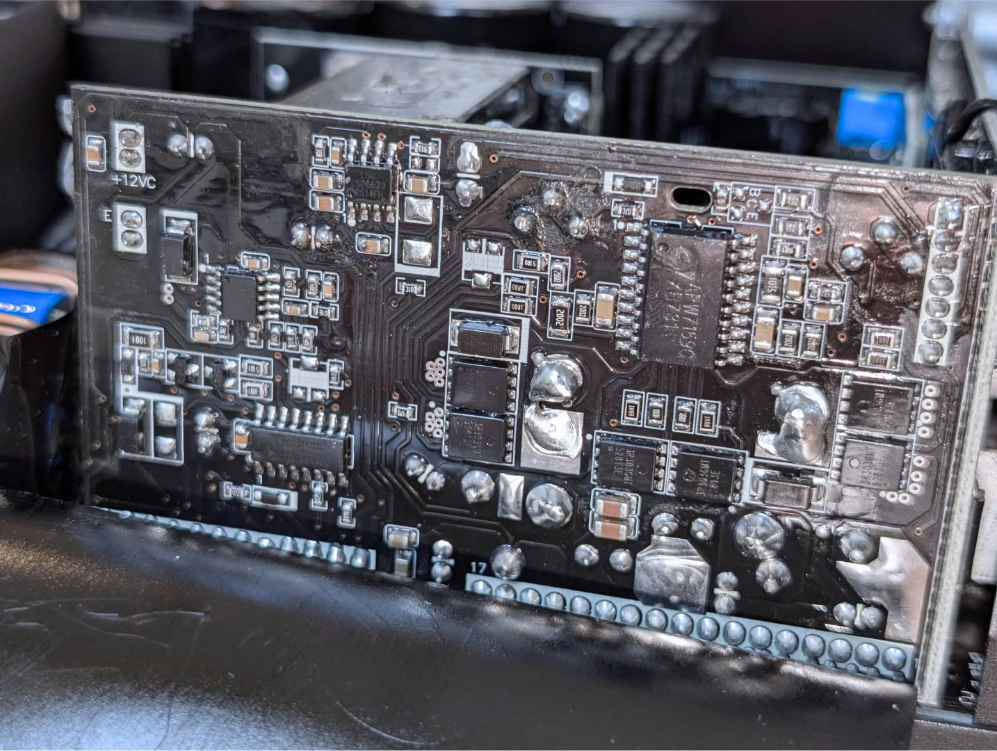
Both sides of the main PCB and all daughterboards have had a conformal coating applied. This process applies a thin clear waterproof layer over the board and components, reducing the risk of damage from moisture, condensation, dust and conductive debris, and allowing operation in conditions up to 95% humidity. It gives a shiny gloss finish.
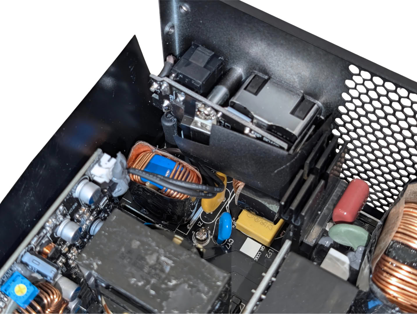
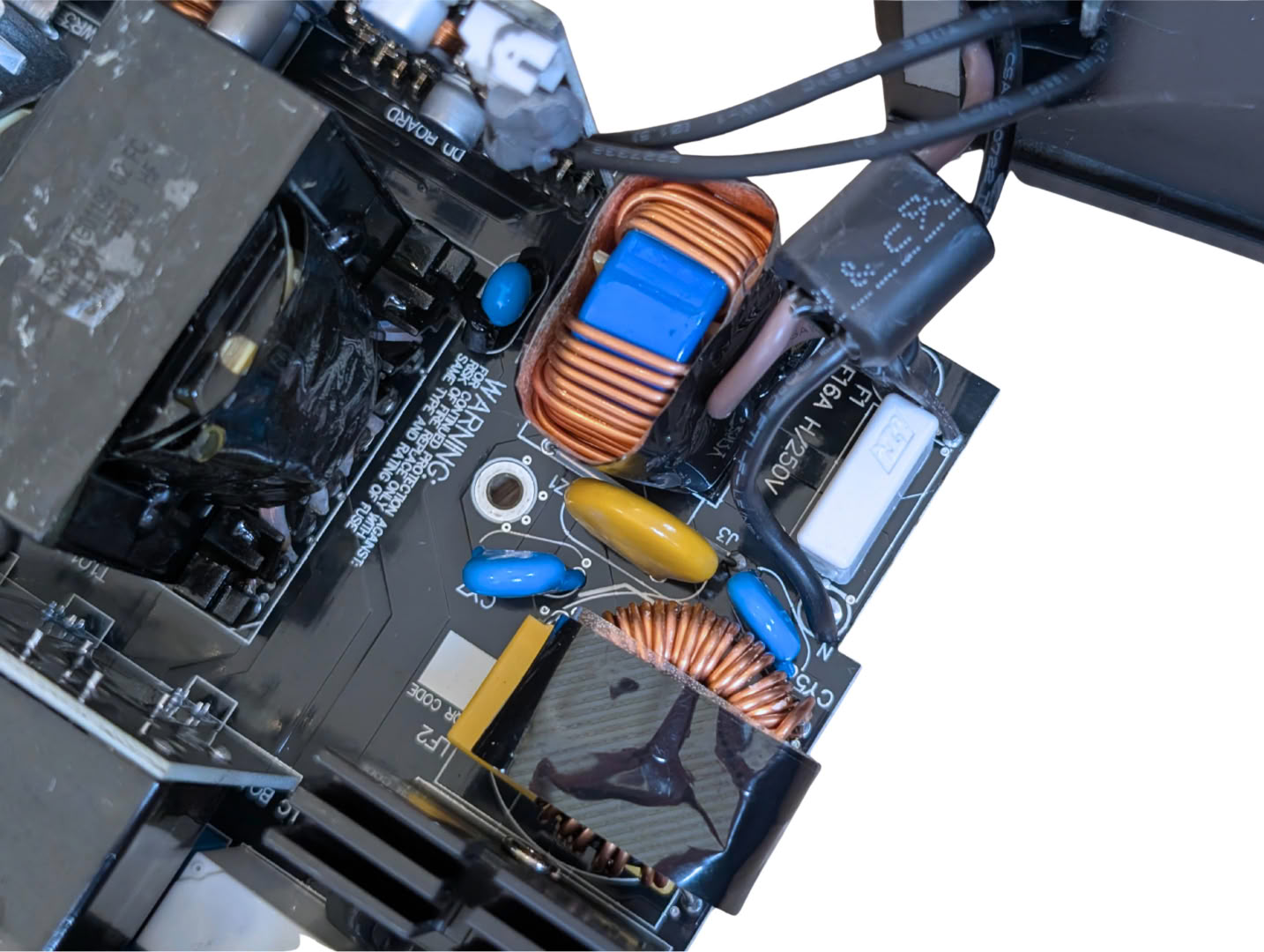
The EMI suppression and transient filtering components are all located on the main board, as opposed to soldered directly to the connector as seen in other devices. There are 2 Y caps, 3 X caps, 2 CM chokes and 1 MOV. There is a small grounded metal strip over the rear of the power terminal.
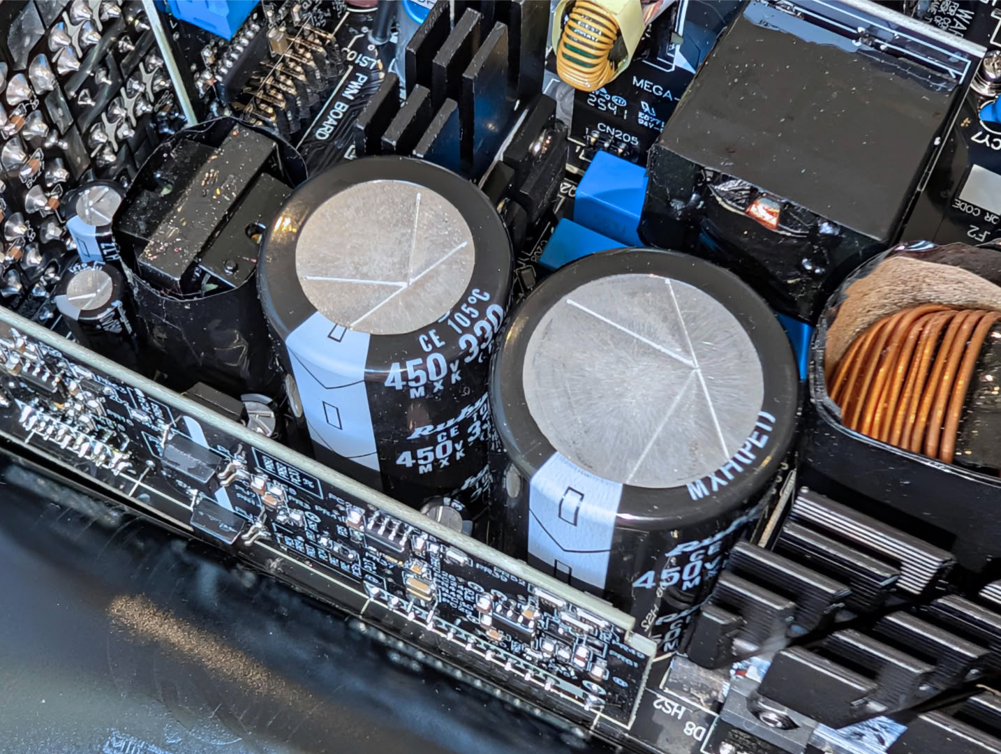
A pair of 420 V 105C Rubycon caps are used for bulk in parallel here, giving a total of 800 uF.
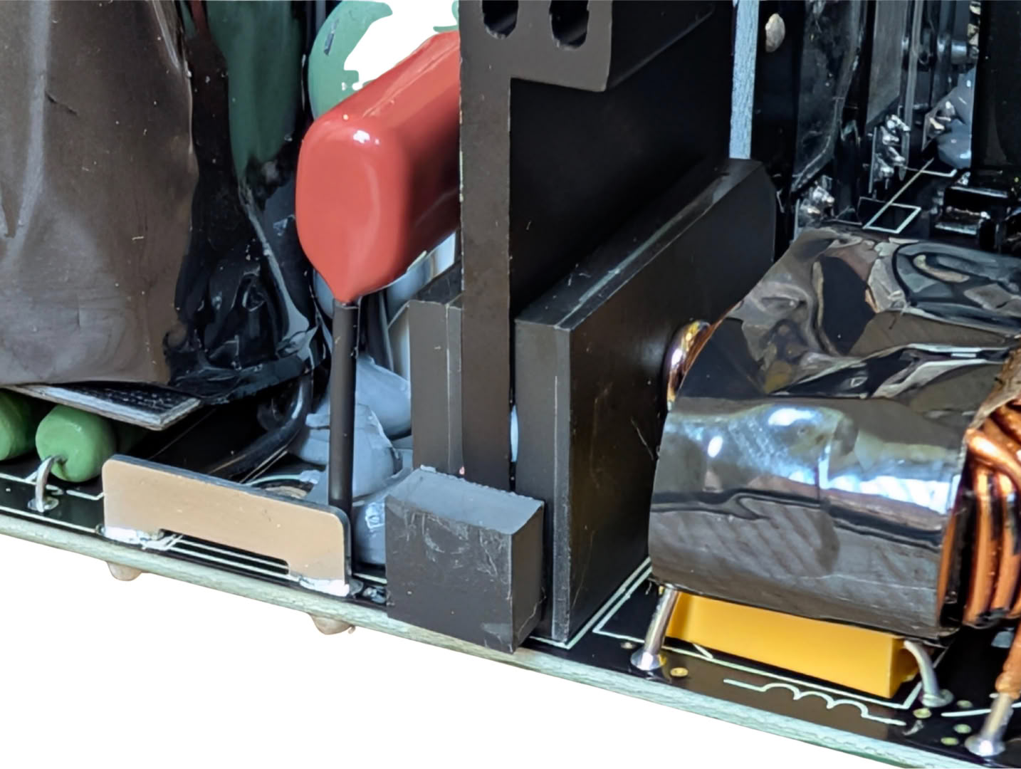
There are a pair of single package full bridge rectifiers sandwiching a heatsink, which is plentiful headroom.
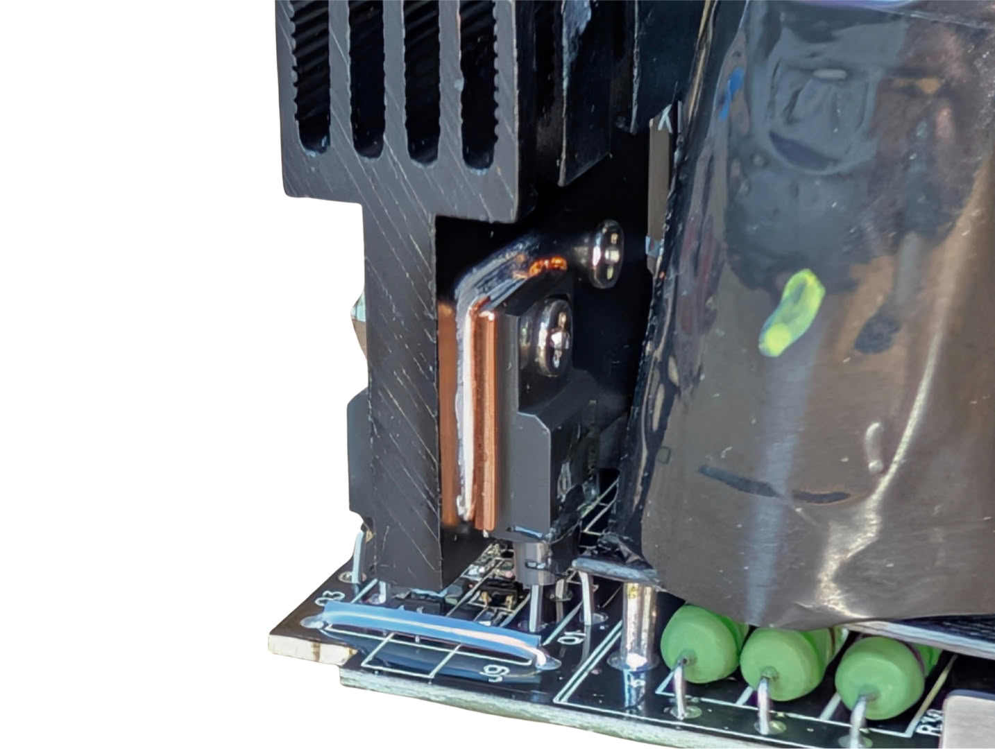
Power factor correction is being handled by an Infineon ICE2PCS02G controller alongside these TO-220 package components on the heatsink.
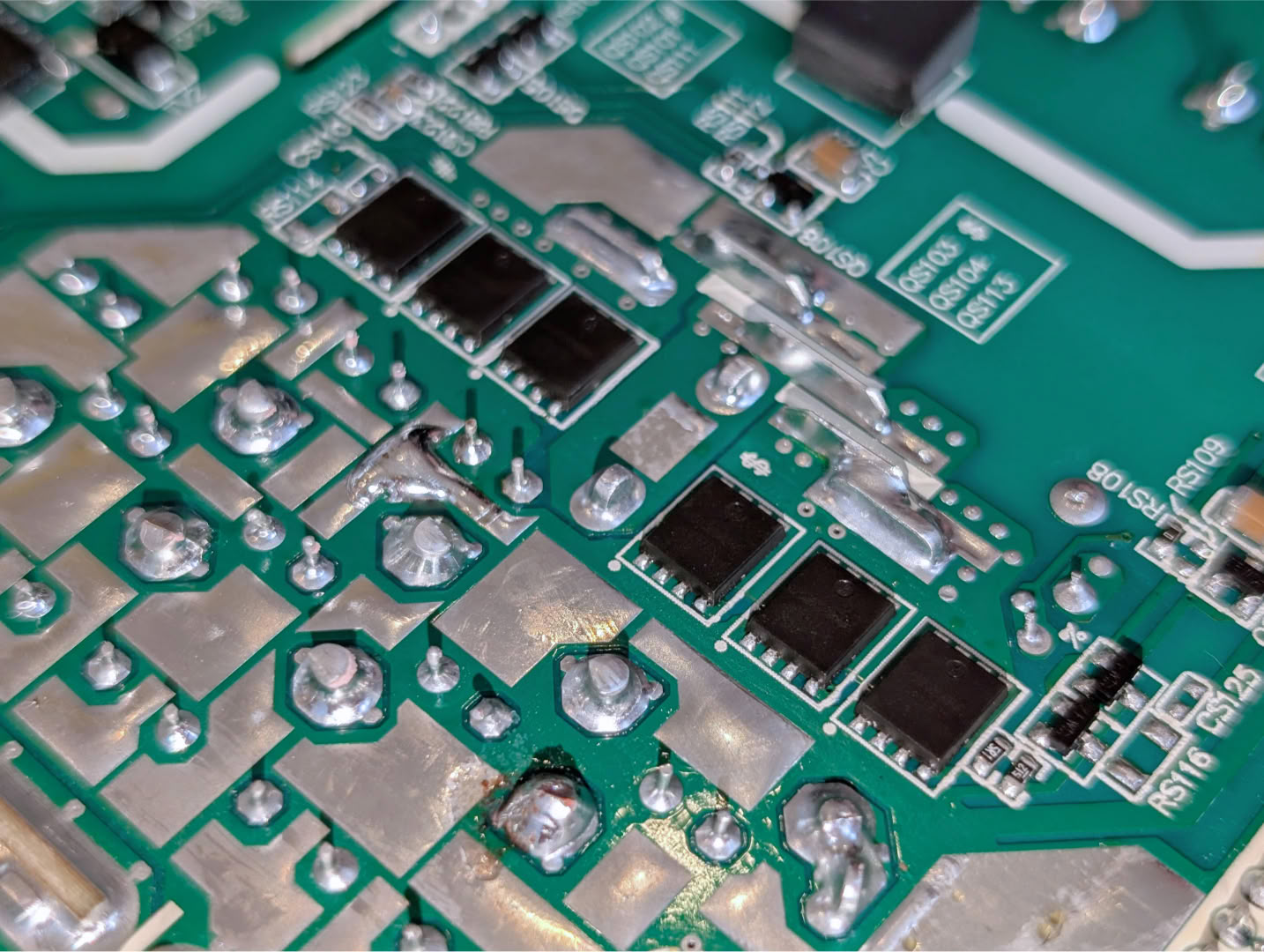
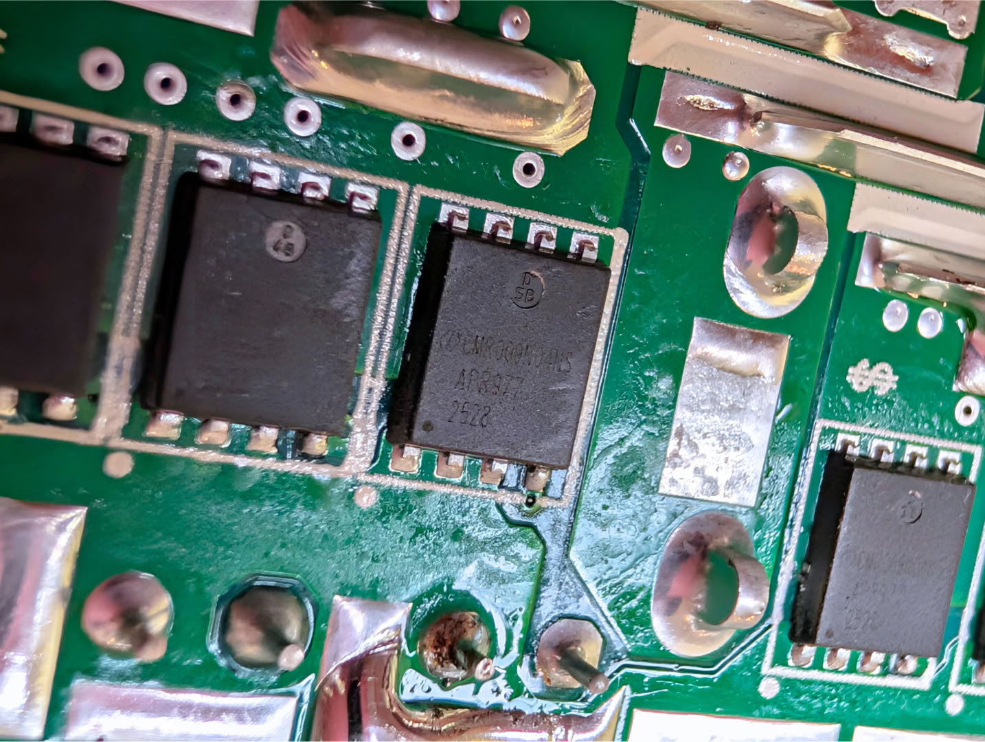
The MOSFETs used for the 12 V rail are marked CMR009N04NF2S. This is likely a clone/remanufacture of the Infineon IPF009N04NF2S but manufactured by CMR (Central Semiconductor). These are 40 V StrongIRFETs, with an RDS of 0.9mΩ and ID of 302 A, 6 are used here in banks of 3.
Heat is wicked away from the MOSFETs by the PCB itself, and by these basic finned heatsinks soldered to the main drain trace, and also through the thermal pad on the underside of the board to the main casing.
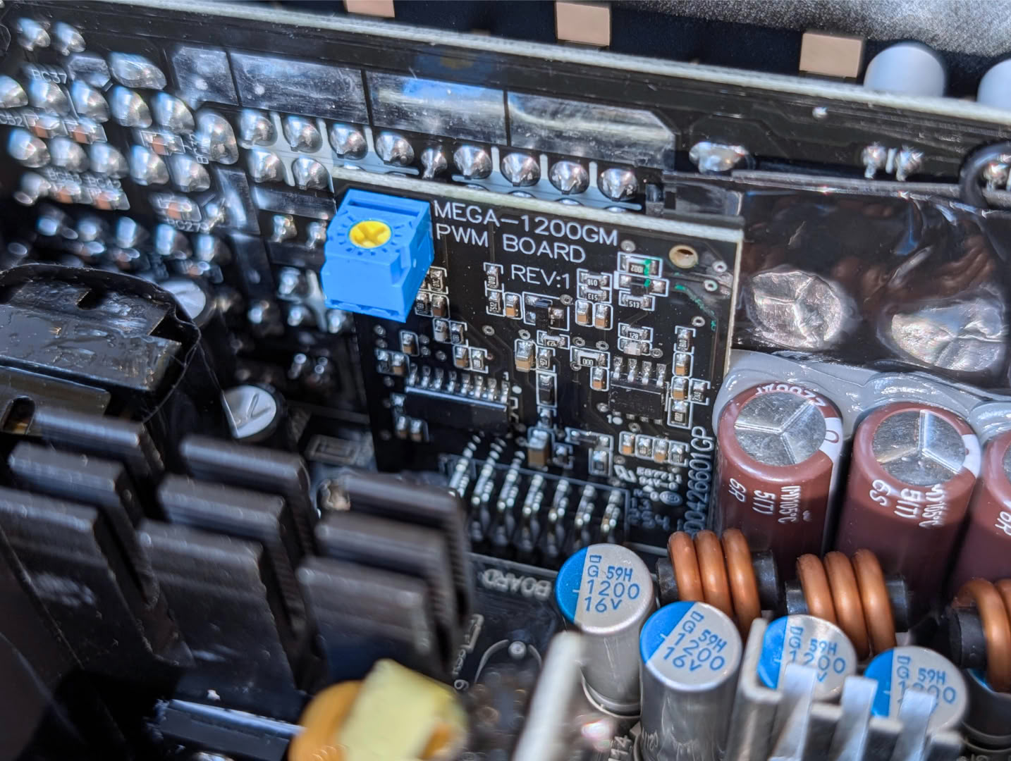
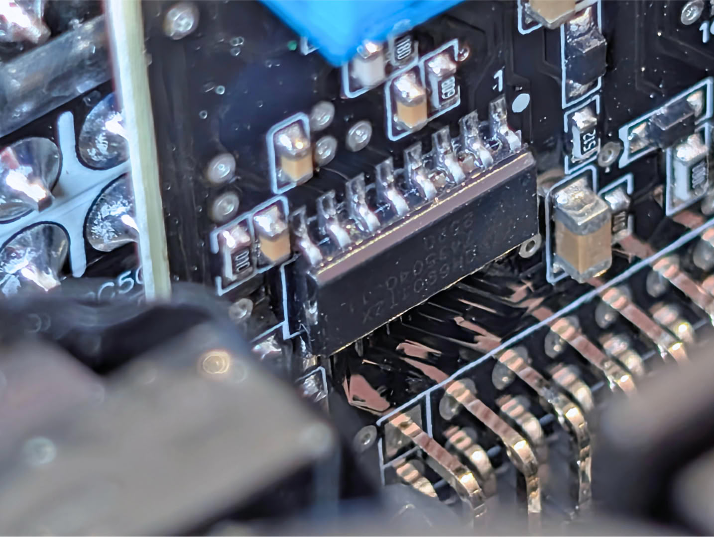
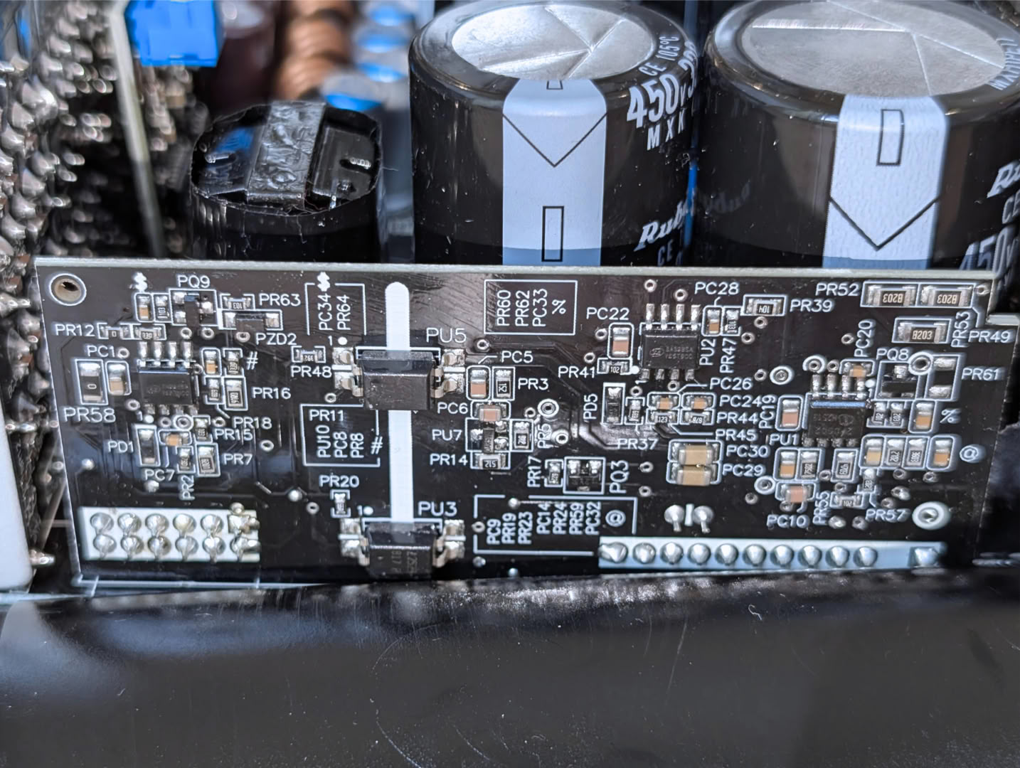
Driving the MOSFETs is this PWM card, with a CM6901 at the heart of it.
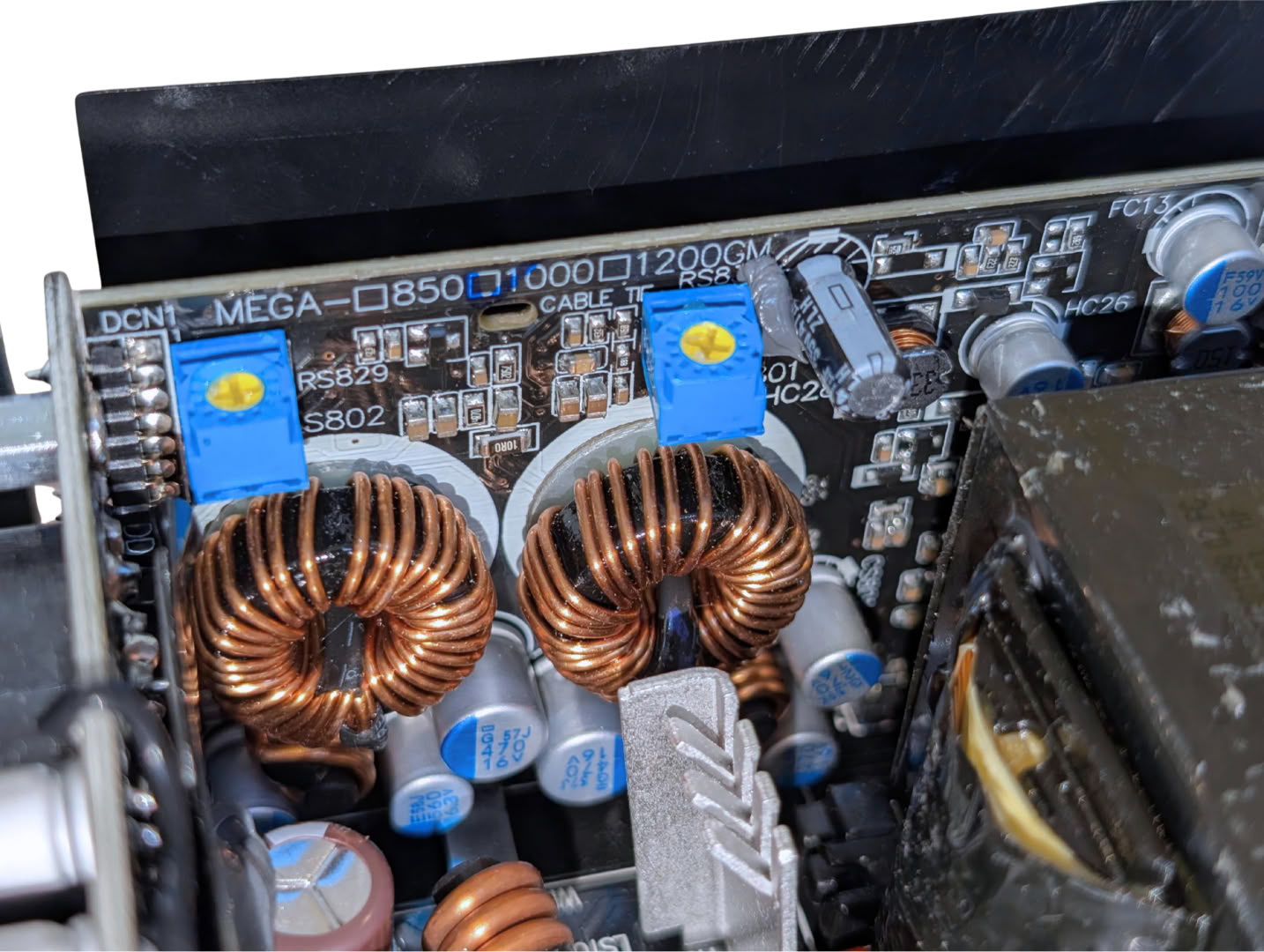
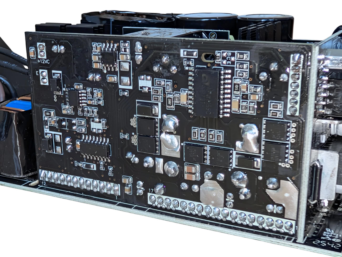
There is a dual-sided daughterboard responsible for stepping down to the lower voltage rails, running XSEMI XP3R303GMT MOSFETs and inductors with an ANPEC APW7159C as the PWM controller. The Weltrend WT7527RA supervisor is also situated on the rear of this board, along with the fan controller.
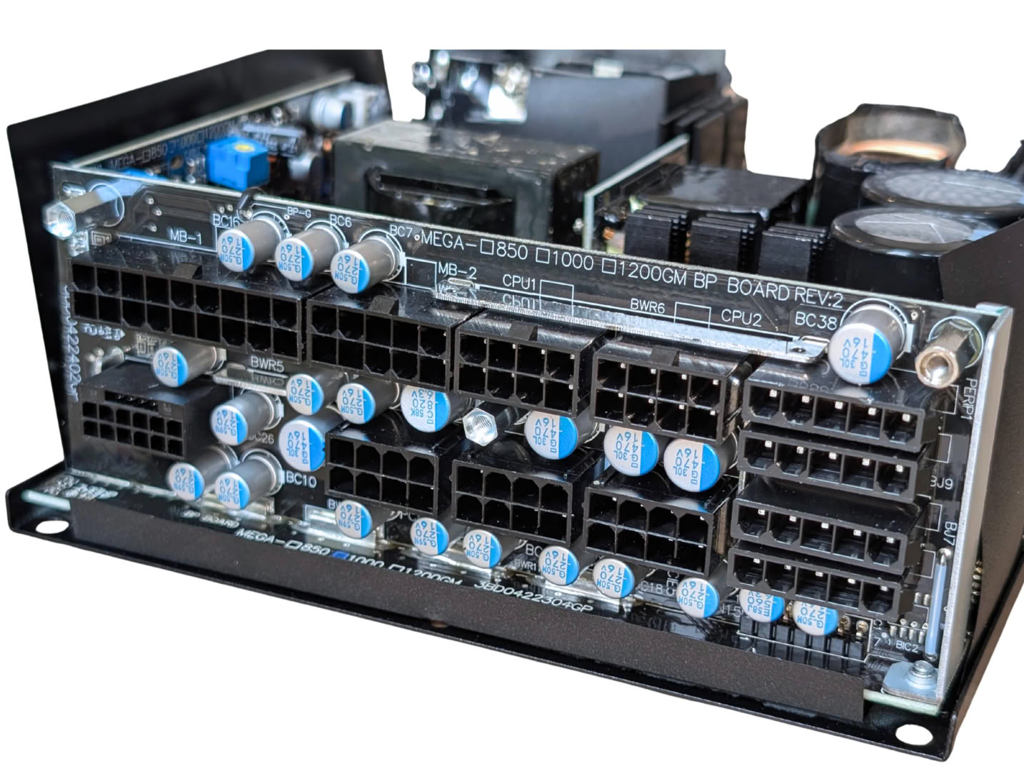
There are plenty of smoothing caps directly next to the power connectors.
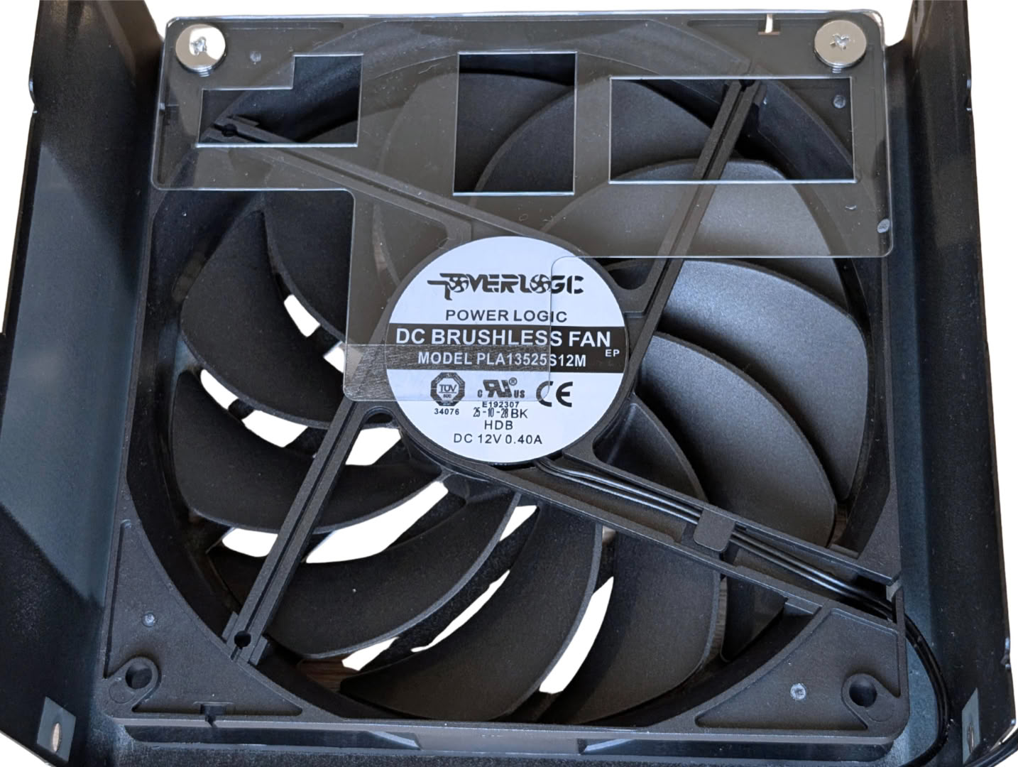
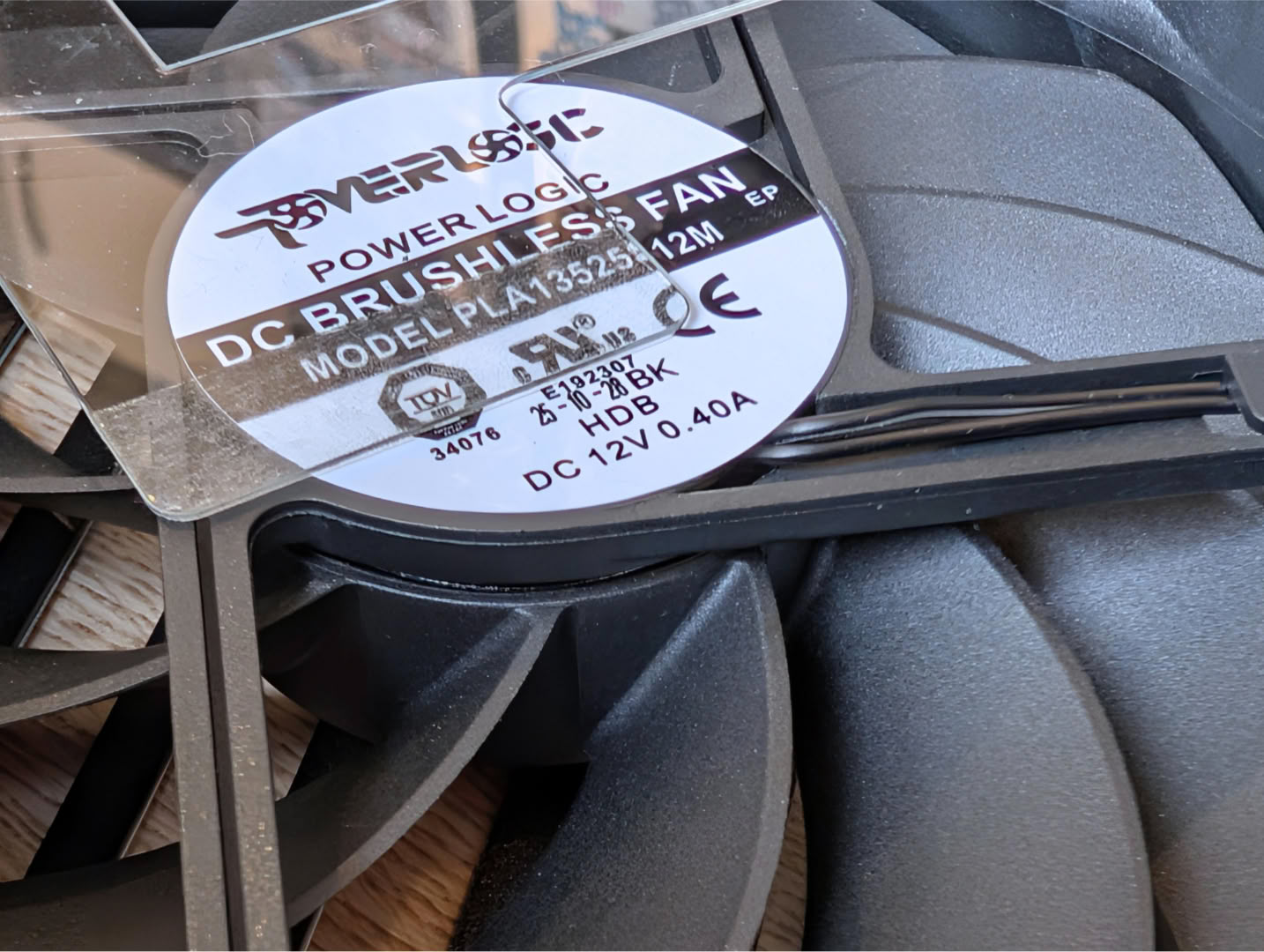
The 135 mm fan being used is a Power Logic PLA13525S12M, taking 0.4 A at full speed and using a Hydro Dynamic Bearing.
Nov 20th, 2026 13:47 PST
change timezone
Latest GPU Drivers
New Forum Posts
- Honestly, do you care about GTA VI? (208)
- When you could finally run Crysis maxed out? (63)
- WarpCoreBench scores! (80)
- GTA VI (20)
- Anthrophics IPO (25)
- GeekMagic Ultra Smart WiFi Weather Station (8)
- Very unusual two gaming-pc scenarios. (35)
- Can i play GTA 6 now? (Joke) (14)
- How to prevent OLED burn damage due to PC freezes or power outtages? (47)
- Zen 3 IF/IMC degradation (239)
Popular Reviews
- AMD Zen 6 Technical Deep Dive
- Ugreen NASync DXP4800 GT Review
- Microsoft Surface Laptop Ultra Review - The Next-gen Arm Laptop
- Corsair RM1200e (Second Generation) Review
- Acemagic Retro X3 Review
- Upcoming Hardware Launches 2027 (Updated Nov 2026)
- Pulsar Office Tour & First Look at P1 Dual-Sensor Mouse
- Biwin Black Opal NV7400 2 TB Review
- AMD Ryzen 7 9800X3D Memory Performance Scaling
- AMD Ryzen 7 9800X3D Review - The Best Gaming Processor
TPU on YouTube
Controversial News Posts
- NVIDIA Co-Founder and CEO Jensen Huang Officially Resigns (490)
- Report: Jensen Huang Eyes NVIDIA Comeback (255)
- Open Letter Asking NVIDIA to Reinstate Jensen Huang Passes 115,000 Signatures (184)
- OpenAI CEO Argues Home PCs Waste the World's Limited DRAM Supply (152)
- NVIDIA Launches Investigation Into Jensen Huang's Relationship With Suspected Chinese Spy (136)
- Intel "Raptor Lake Next" 16-Core and 20-Core CPUs Surface (130)
- Legendary Game Studio BioWare Shuts Down Following EA Layoffs (104)
- Dell CEO Says the Memory Shortage Will Get Worse in 2027 (95)