 25
25
Gainward GeForce RTX 4070 Ti Super Phoenix GS Review
(25 Comments) »Introduction
Gainward GeForce RTX 4070 Ti SUPER Phoenix GS is a new performance segment graphics card based on NVIDIA's latest high-end GPU. The new RTX 4070 Ti SUPER comes from a three-part mid-lifecycle refresh of the RTX 40-series Ada generation, focusing mainly on the higher end of the product stack. The RTX 4070 Ti SUPER is recommended by NVIDIA for 1440p high refresh-rate gaming with maxed out settings and ray tracing. The RTX 4070 series of graphics cards are very much capable of gameplay at 4K Ultra HD, if you're a little careful with your game settings, or use features such as DLSS that come with pretty much every new AAA title these days; or even the newer DLSS 3 Frame Generation, which nearly doubles frame-rates by drawing alternate frames entirely using AI.

The new GeForce RTX 4070 Ti SUPER replaces the RTX 4070 Ti from the product stack, at its $800 price-point, which is now no longer in production, and will be phased out of the market at lower prices. The RTX 4070 Ti SUPER comes with significantly upgraded specifications, most notably, its increased 16 GB of memory across a wider 256-bit memory bus; as opposed to 12 GB over 192-bit for the original RTX 4070 Ti. This is a straight 33% increase in memory bandwidth and size. The extra 4 GB of memory is what makes us excited about this card's prospects with 4K gaming. Besides the extra memory, the RTX 4070 Ti SUPER gets 10% more shaders, and 20% more ROPs. All this comes from NVIDIA's switch to the larger AD103 silicon from the AD104 that had been maxed out to create the RTX 4070 Ti.
NVIDIA carved the RTX 4070 Ti SUPER out of the AD103 by enabling 66 out of 80 SM, worth 8,448 CUDA cores; 264 Tensor cores, 66 RT cores, and 264 TMUs. NVIDIA enabled 96 out of the 112 ROPs present on the silicon, which is still a big uplift from the 80 on the RTX 4070 Ti; although the on-die L2 cache size remains the same at 48 MB out of the 64 MB available on the silicon. The GPU runs at 2610 MHz boost, and the memory at 21 Gbps, which is lower than the 22.5 Gbps of the RTX 4080, but still results in a 33% higher memory bandwidth when compared to the RTX 4070 Ti, thanks to that 256-bit memory bus.
The SUPER moniker only represents performance uplifts at existing price-points, no new features are introduced. The RTX 4070 Ti SUPER is still based on the existing Ada Lovelace graphics architecture. Ada introduces a new generation CUDA core with increased IPC and support for new math formats, as well as shader execution reordering, a feature that speeds up ray tracing. The new 3rd generation RT core, besides increased ray intersection performance, debuts displaced micro-meshes, which enables greater complexity in ray traced objects. The new optical flow accelerator component enables the GPU to draw alternate frames entirely using AI, cutting out the main raster machinery, which is how DLSS 3 Frame Generation works.
Gainward's GS line of graphics cards go all the way back to the GeForce 4 Ti days, where it represented "Golden Sample," the company's highest state of factory OC. On the RTX 4070 Ti SUPER, some 15 generations ahead, the Gainward GS brand means overclocked speeds of 2670 MHz, compared to 2610 MHz reference. The Gainward RTX 4070 Ti SUPER Phoenix features a simple triple-slot, cooling solution with a triple fan setup. Gainward hasn't given out a price, but we are estimating a price of $870, which is what we are using in our cost-performance calculations.
Short 10-Minute Video Comparing 10x RTX 4070 Ti Super
Our goal with the videos is to create short summaries, not go into all the details and test results, which can be found in our written reviews.
| Price | Cores | ROPs | Core Clock | Boost Clock | Memory Clock | GPU | Transistors | Memory | |
|---|---|---|---|---|---|---|---|---|---|
| RTX 3070 Ti | $350 | 6144 | 96 | 1575 MHz | 1770 MHz | 1188 MHz | GA104 | 17400M | 8 GB, GDDR6X, 256-bit |
| RX 6800 | $450 | 3840 | 96 | 1815 MHz | 2105 MHz | 2000 MHz | Navi 21 | 26800M | 16 GB, GDDR6, 256-bit |
| RX 7700 XT | $430 | 3456 | 96 | 2171 MHz | 2544 MHz | 2250 MHz | Navi 32 | 26500M | 12 GB, GDDR6, 192-bit |
| RX 6800 XT | $500 | 4608 | 128 | 2015 MHz | 2250 MHz | 2000 MHz | Navi 21 | 26800M | 16 GB, GDDR6, 256-bit |
| RTX 3080 | $450 | 8704 | 96 | 1440 MHz | 1710 MHz | 1188 MHz | GA102 | 28000M | 10 GB, GDDR6X, 320-bit |
| RTX 4070 | $540 | 5888 | 64 | 1920 MHz | 2475 MHz | 1313 MHz | AD104 | 35800M | 12 GB, GDDR6X, 192-bit |
| RX 7800 XT | $500 | 3840 | 96 | 2124 MHz | 2430 MHz | 2425 MHz | Navi 32 | 28100M | 16 GB, GDDR6, 256-bit |
| RX 6900 XT | $650 | 5120 | 128 | 2015 MHz | 2250 MHz | 2000 MHz | Navi 21 | 26800M | 16 GB, GDDR6, 256-bit |
| RX 6950 XT | $630 | 5120 | 128 | 2100 MHz | 2310 MHz | 2250 MHz | Navi 21 | 26800M | 16 GB, GDDR6, 256-bit |
| RTX 3090 | $800 | 10496 | 112 | 1395 MHz | 1695 MHz | 1219 MHz | GA102 | 28000M | 24 GB, GDDR6X, 384-bit |
| RTX 4070 Super | $600 | 7168 | 80 | 1980 MHz | 2475 MHz | 1313 MHz | AD104 | 35800M | 12 GB, GDDR6X, 192-bit |
| RTX 4070 Ti | $750 | 7680 | 80 | 2310 MHz | 2610 MHz | 1313 MHz | AD104 | 35800M | 12 GB, GDDR6X, 192-bit |
| RTX 4070 Ti Super | $800 | 8448 | 112 | 2340 MHz | 2610 MHz | 1313 MHz | AD103 | 45900M | 16 GB, GDDR6X, 256-bit |
| Gainward RTX 4070 Ti Super Phoenix GS | $870 | 8448 | 112 | 2340 MHz | 2670 MHz | 1313 MHz | AD103 | 45900M | 16 GB, GDDR6X, 256-bit |
| RX 7900 XT | $710 | 5376 | 192 | 2000 MHz | 2400 MHz | 2500 MHz | Navi 31 | 57700M | 20 GB, GDDR6, 320-bit |
| RTX 3090 Ti | $1050 | 10752 | 112 | 1560 MHz | 1950 MHz | 1313 MHz | GA102 | 28000M | 24 GB, GDDR6X, 384-bit |
| RTX 4080 | $1200 | 9728 | 112 | 2205 MHz | 2505 MHz | 1400 MHz | AD103 | 45900M | 16 GB, GDDR6X, 256-bit |
| RTX 4080 Super | $1000 | 10240 | 112 | 2295 MHz | 2550 MHz | 1400 MHz | AD103 | 45900M | 16 GB, GDDR6X, 256-bit |
| RX 7900 XTX | $970 | 6144 | 192 | 2300 MHz | 2500 MHz | 2500 MHz | Navi 31 | 57700M | 24 GB, GDDR6, 384-bit |
| RTX 4090 | $2000 | 16384 | 176 | 2235 MHz | 2520 MHz | 1313 MHz | AD102 | 76300M | 24 GB, GDDR6X, 384-bit |
Architecture
The Ada graphics architecture heralds the third generation of the NVIDIA RTX technology, an effort toward increasing the realism of game visuals by leveraging real-time ray tracing, without the enormous amount of compute power required to draw purely ray-traced 3D graphics. This is done by blending conventional raster graphics with ray traced elements such as reflections, lighting, and global illumination, to name a few. The 3rd generation of RTX introduces the new higher IPC "Ada" CUDA core, 3rd generation RT core, 4th generation Tensor core, and the new Optical Flow Processor, a component that plays a key role in generating new frames without involving the GPU's main graphics rendering pipeline. The GeForce Ada graphics architecture driving the RTX 4070 Ti SUPER leverages the TSMC 5 nm EUV foundry process to increase transistor counts.

The GeForce RTX 4070 Ti SUPER gets a significant memory sub-system uplift over the original RTX 4070 Ti, besides an increase in shaders and other on-die components. Since NVIDIA maxed out the AD104 to create the RTX 4070 Ti, the only way it could go about creating the RTX 4070 Ti SUPER is by tapping into the larger AD103 that powers the RTX 4080 and the upcoming RTX 4080 SUPER. The biggest perks of the switch to AD103 is its wider 256-bit memory bus, which allowed NVIDIA to increase the memory from 12 GB to 16 GB.
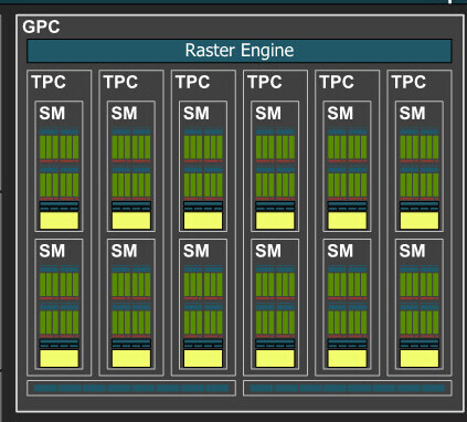
The AD103 die is built on the 5 nm EUV foundry process, with a die size of 379 mm² and 45.9 billion transistors. The chip features a PCI-Express 4.0 x16 host interface along with support for PCI resizable BAR; and its 256-bit wide GDDR6X memory interface. The GigaThread Engine serves as the main workflow controller for the GPU, dispatching work among the GPU's 7 graphics processing clusters (GPCs). Each GPC shares a Raster Engine and render backends among six texture processing clusters (TPCs), the indivisible subunit of the GPU. Each of these has two Streaming Multiprocessors (SM), and a Polymorph unit. Each SM contains 128 CUDA cores across four partitions. Half of these CUDA cores are pure-FP32; while the other half is capable of FP32 or INT32. The SM retains concurrent FP32+INT32 math processing capability. The SM also contains a 3rd generation RT core, four 4th generation Tensor cores, some cache memory, and four TMUs. One of the seven GPCs on the AD103 physically only has four TPCs.
With a total of 40 TPCs, or 80 SM, AD103 physically features 10,240 CUDA cores, 320 Tensor cores, 80 RT cores, and 320 TMUs; along with 64 MB of on-die L2 cache, and 112 ROPs. NVIDIA carved the RTX 4070 Ti SUPER out of the AD103 by enabling 66 out of 80 SM, 48 MB out of the 64 MB of L2 cache present; and 96 ROPs out of the 112 present. This results in 8,448 CUDA cores, 264 Tensor cores, 66 RT cores, 264 TMUs, 96 ROPs, and 48 MB of L2 cache. NVIDIA also disabled a few NVDEC units, giving this the same exact video acceleration configuration as the RTX 4070 Ti, with two NVENC and one NVDEC units. The 256-bit memory interface drives 16 GB of memory, however the memory runs at 21 Gbps, compared to the 22.5 Gbps of the RTX 4080, and 23 Gbps of the upcoming RTX 4080 SUPER. Even with 21 Gbps, the memory bandwidth on tap is an impressive 672 GB/s, a 33% increase over that of the original RTX 4070 Ti.
3rd Gen RT Core and Ray Tracing


The 3rd generation RT core accelerates the most math-intensive aspects of real-time ray tracing, including BVH traversal. Displaced micro-mesh engine is a revolutionary feature introduced with the new 3rd generation RT core. Just as mesh shaders and tessellation have had a profound impact on improving performance with complex raster geometry, allowing game developers to significantly increase geometric complexity; DMMs is a method to reduce the complexity of the bounding-volume hierarchy (BVH) data-structure, which is used to determine where a ray hits geometry. Previously, the BVH had to capture even the smallest details to properly determine the intersection point. Ada's ray tracing architecture also receives a major performance uplift from Shader Execution Reordering (SER), a software-defined feature that requires awareness from game-engines, to help the GPU reorganize and optimize worker threads associated with ray tracing.


The BVH now needn't have data for every single triangle on an object, but can represent objects with complex geometry as a coarse mesh of base triangles, which greatly simplifies the BVH data structure. A simpler BVH means less memory consumed and helps to greatly reduce ray tracing CPU load, because the CPU only has to generate a smaller structure. With older "Ampere" and "Turing" RT cores, each triangle on an object had to be sampled at high overhead, so the RT core could precisely calculate ray intersection for each triangle. With Ada, the simpler BVH, plus the displacement maps can be sent to the RT core, which is now able to figure out the exact hit point on its own. NVIDIA has seen 11:1 to 28:1 compression in total triangle counts. This reduces BVH compile times by 7.6x to over 15x, in comparison to the older RT core; and reducing its storage footprint by anywhere between 6.5 to 20 times. DMMs could reduce disk- and memory bandwidth utilization, utilization of the PCIe bus, as well as reduce CPU utilization. NVIDIA worked with Simplygon and Adobe to add DMM support for their tool chains.
Opacity Micro Meshes

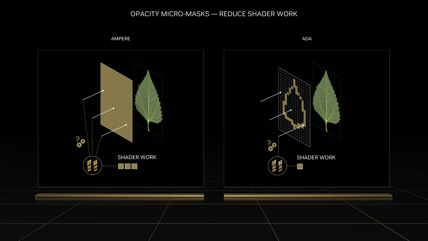
Opacity Micro Meshes (OMM) is a new feature introduced with Ada to improve rasterization performance, particularly with objects that have alpha (transparency data). Most low-priority objects in a 3D scene, such as leaves on a tree, are essentially rectangles with textures on the leaves where the transparency (alpha) creates the shape of the leaf. RT cores have a hard time intersecting rays with such objects, because they're not really in the shape that they appear (they're really just rectangles with textures that give you the illusion of shape). Previous-generation RT cores had to have multiple interactions with the rendering stage to figure out the shape of a transparent object, because they couldn't test for alpha by themselves.
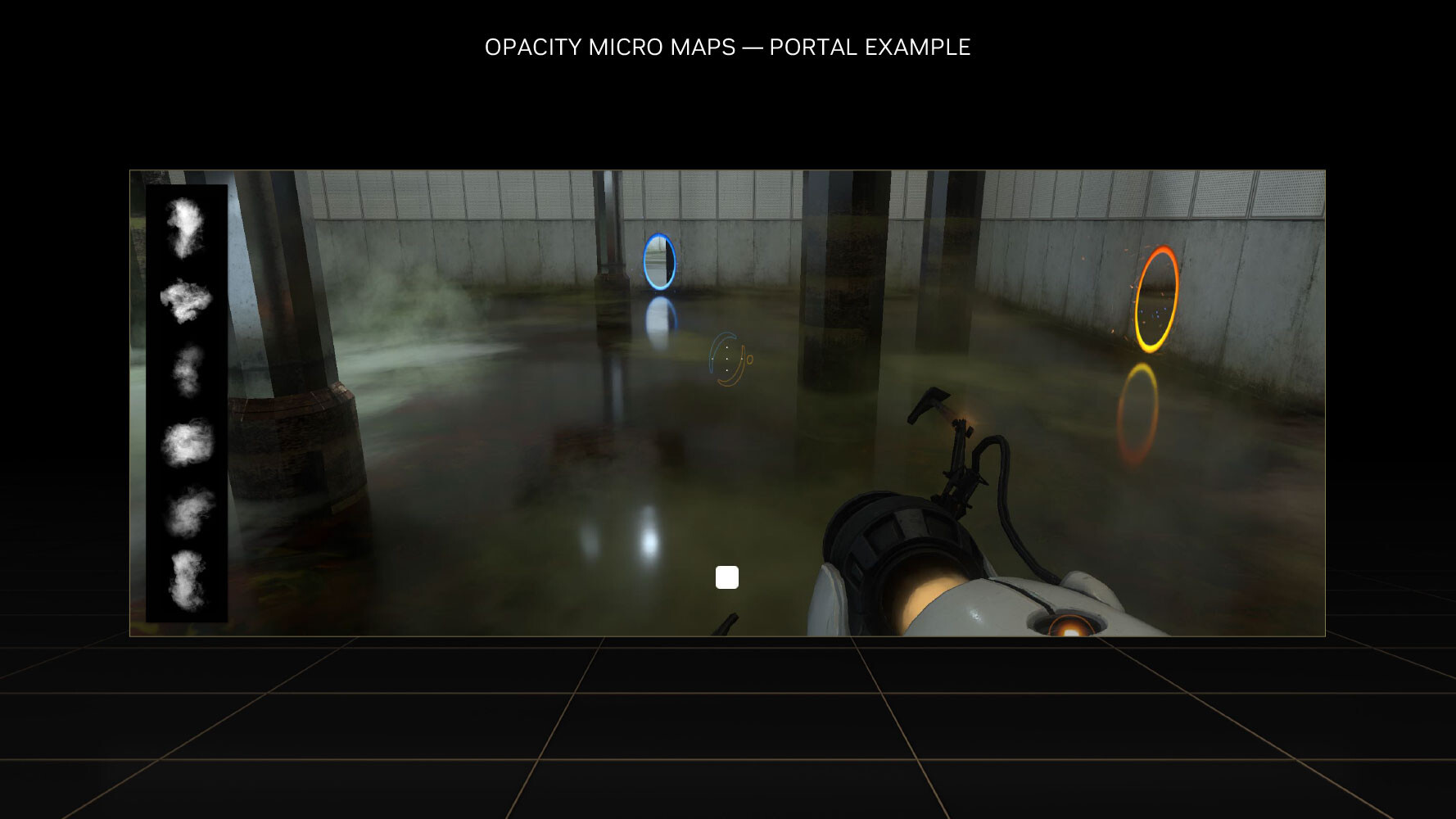

This has been solved by using OMMs. Just as DMMs simplify geometry by creating meshes of micro-triangles; OMMs create meshes of rectangular textures that align with parts of the texture that aren't alpha, so the RT core has a better understanding of the geometry of the object, and can correctly calculate ray intersections. This has a significant performance impact on shading performance in non-RT applications, too. Practical applications of OMMs aren't just low-priority objects such as vegetation, but also smoke-sprites and localized fog. Traditionally there was a lot of overdraw for such effects, because they layered multiple textures on top of each other, that all had to be fully processed by the shaders. Now only the non-opaque pixels get executed—OMMs provide a 30 percent speedup with graphics buffer fill-rates, and a 10 percent impact on frame-rates.
DLSS 3 Frame Generation


DLSS 3 introduces a revolutionary new feature that promises a doubling in frame-rate at comparable quality, it's called AI frame-generation. Building on DLSS 2 and its AI super-resolution (scaling up a lower-resolution frame to native resolution with minimal quality loss); DLSS 3 can generate entire frames simply using AI, without involving the graphics rendering pipeline, it's also possible to enable frame generation at native resolution without upscaling. Later in the article, we will show you DLSS 3 in action.


Every alternating frame with DLSS 3 is hence AI-generated, without being a replica of the previous rendered frame. This is possible only on the Ada graphics architecture, because of a hardware component called the optical flow accelerator (OFA), which assists in predicting what the next frame could look like, by creating what NVIDIA calls an optical flow-field. OFA ensures that the DLSS 3 algorithm isn't confused by static objects in a rapidly-changing 3D scene (such as a race sim). The process heavily relies on the performance uplift introduced by the FP8 math format of the 4th generation Tensor core. A third key ingredient of DLSS 3 is Reflex. By reducing the rendering queue to zero, Reflex plays a vital role in ensuring that latency with DLSS 3 enabled is at an acceptable level. A combination of OFA and the 4th Gen Tensor core is why the Ada architecture is required to use DLSS 3, and why it won't work on older architectures.
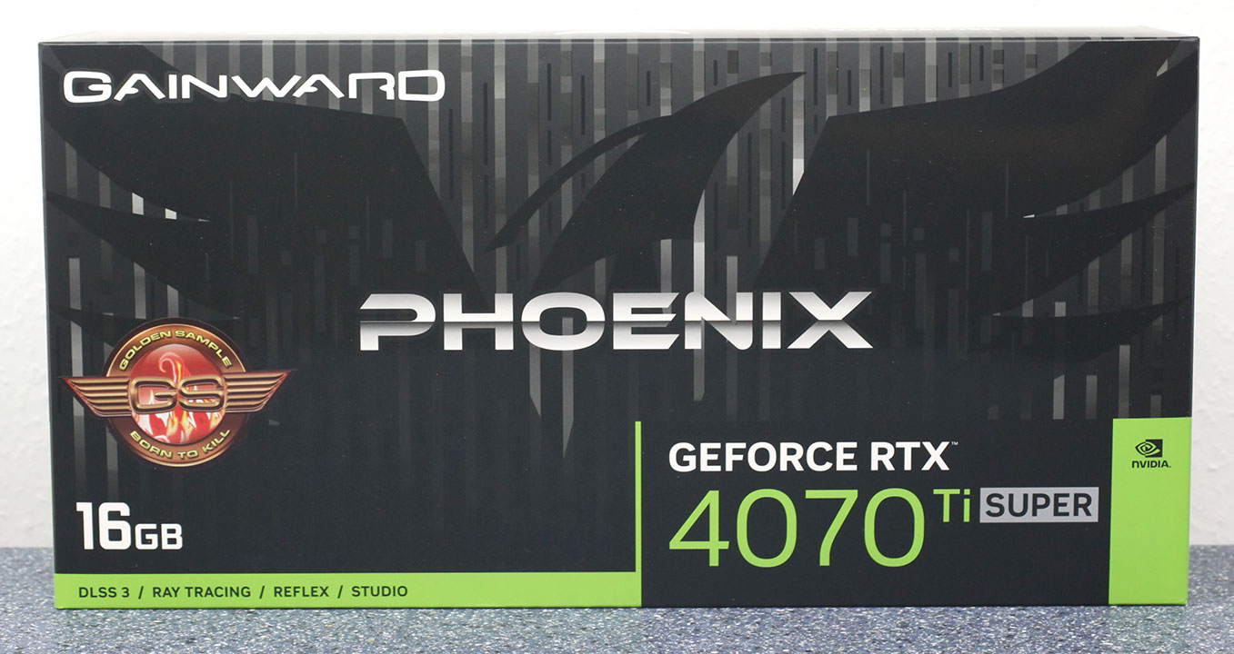
Packaging

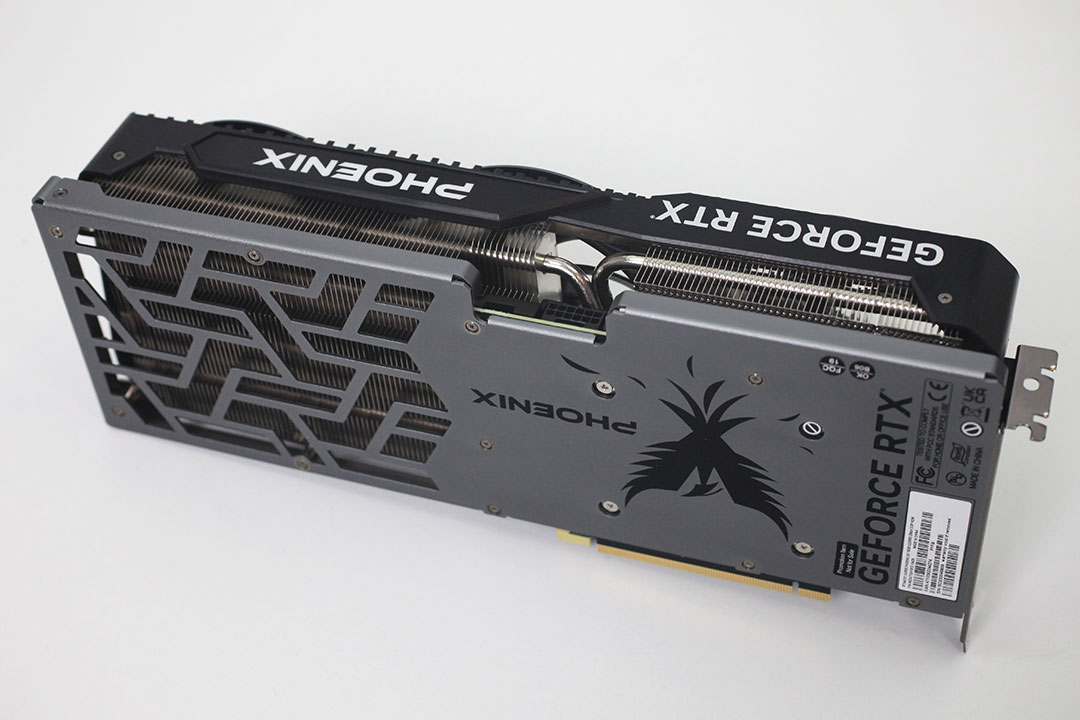
The Card

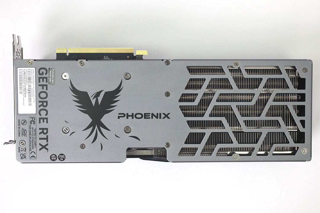
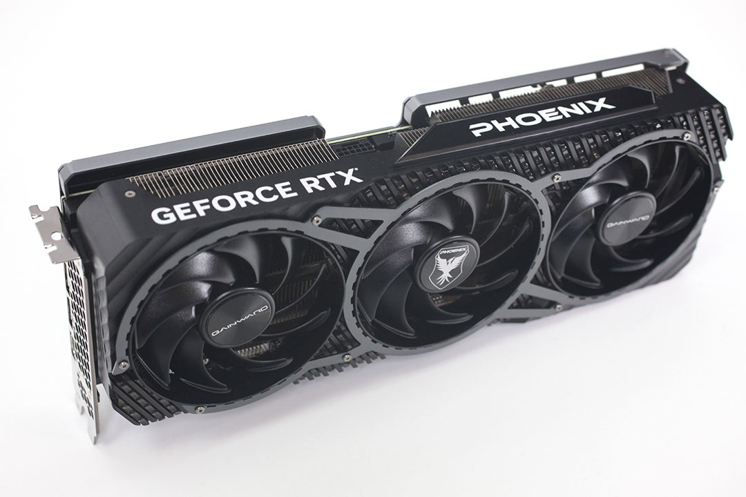
Gainward's cards comes with a complex industrial look on the main cooler, maybe reminding me a bit of alien structures in sci-fi movies. On the back you get a high-quality metal backplate, the front cooler shroud is made from plastic.


Dimensions of the card are 33.0 x 13.0 cm, and it weighs 1521 g.

Installation requires three slots in your system. We measured the card's width to be 66 mm.

Display connectivity includes three standard DisplayPort 1.4a ports and one HDMI 2.1a (same as Ampere and same as non-Super Ada).
NVIDIA introduced the concept of dual NVDEC and NVENC Codecs with the Ada Lovelace architecture. This means there are two independent sets of hardware-accelerators; so you can encode and decode two streams of video in parallel or one stream at double the FPS rate. While the RTX 4070 Ti features dual units, the RTX 4070 Super and RTX 4070 come with only one of them. The new 8th Gen NVENC now accelerates AV1 encoding, besides HEVC. You also get an "optical flow accelerator" unit that is able to calculate intermediate frames for videos, to smooth playback. The same hardware unit is used for frame generation in DLSS 3.

All GeForce RTX 4070 Ti Super graphics cards use the 12+4 pin ATX 12VHPWR connector, an adapter cable is included in the box.
Our Patreon Silver Supporters can read articles in single-page format.
May 8th, 2024 05:11 EDT
change timezone
Latest GPU Drivers
New Forum Posts
- TPU's Nostalgic Hardware Club (18498)
- Does anyone here overclock their video cards? Is it really worth it? (32)
- POLL: Can you see the difference past 60fps (gaming/other) (21)
- Your way of cooling your PC? (3)
- High c0% and system idle process (1)
- Free Games Thread (3787)
- Nerdy year long streaming saga [ XD probably] (2)
- I wonder how much performance could be gained with m4 chip in iPad pro OLED, if it had an AirJet (1)
- PSU making a clicking sound, PC wont turn on (14)
- Technical Issues - TPU Main Site & Forum (2024) (54)
Popular Reviews
- CHERRY XTRFY M64 Pro Review
- Corsair iCUE Link RX120 RGB 120 mm Fan Review
- Finalmouse UltralightX Review
- Upcoming Hardware Launches 2023 (Updated Feb 2024)
- Cougar Hotrod Royal Gaming Chair Review
- Meze Audio LIRIC 2nd Generation Closed-Back Headphones Review
- AMD Ryzen 7 7800X3D Review - The Best Gaming CPU
- ASRock NUC BOX-155H (Intel Core Ultra 7 155H) Review
- ASUS Radeon RX 7900 GRE TUF OC Review
- Sapphire Radeon RX 7900 GRE Pulse Review
Controversial News Posts
- Intel Statement on Stability Issues: "Motherboard Makers to Blame" (259)
- AMD to Redesign Ray Tracing Hardware on RDNA 4 (203)
- Windows 11 Now Officially Adware as Microsoft Embeds Ads in the Start Menu (167)
- NVIDIA to Only Launch the Flagship GeForce RTX 5090 in 2024, Rest of the Series in 2025 (137)
- Sony PlayStation 5 Pro Specifications Confirmed, Console Arrives Before Holidays (119)
- AMD's RDNA 4 GPUs Could Stick with 18 Gbps GDDR6 Memory (114)
- NVIDIA Points Intel Raptor Lake CPU Users to Get Help from Intel Amid System Instability Issues (106)
- AMD Ryzen 9 7900X3D Now at a Mouth-watering $329 (104)