 14
14
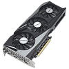
Gigabyte GeForce RTX 3050 Gaming OC Review
Test Setup »High-resolution PCB Pictures
These pictures are for the convenience of volt modders and people who would like to see all the finer details on the PCB. Feel free to link back to us and use these in your articles, videos or forum posts.
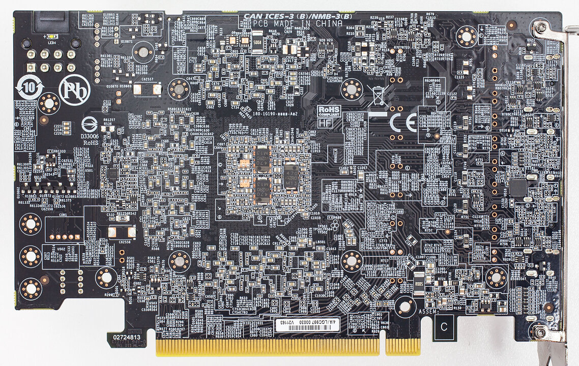
High-res versions are also available (front, back).
Circuit Board (PCB) Analysis
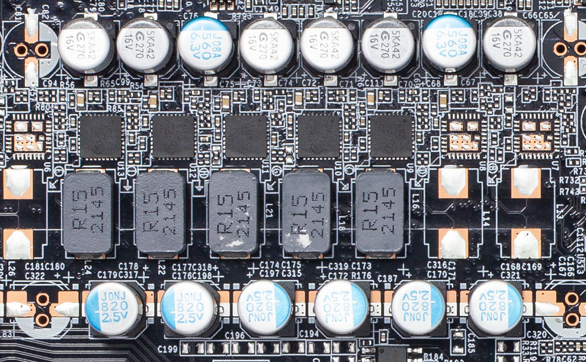
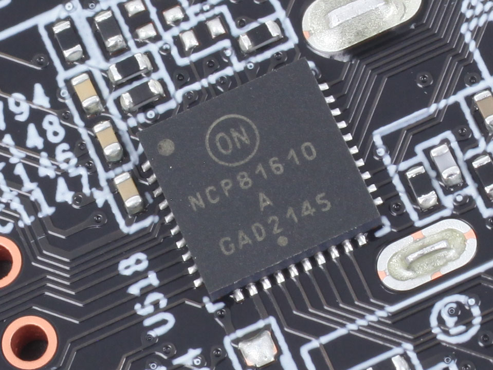
The GPU VRM is a five phase-design controlled by an OnSemi NCP81610 controller.
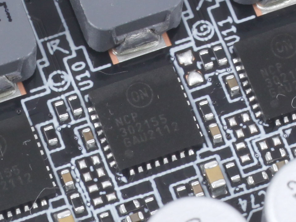
OnSemi NCP302155 DrMOS chips are used for GPU voltage; they are rated for up to 55 A output current.
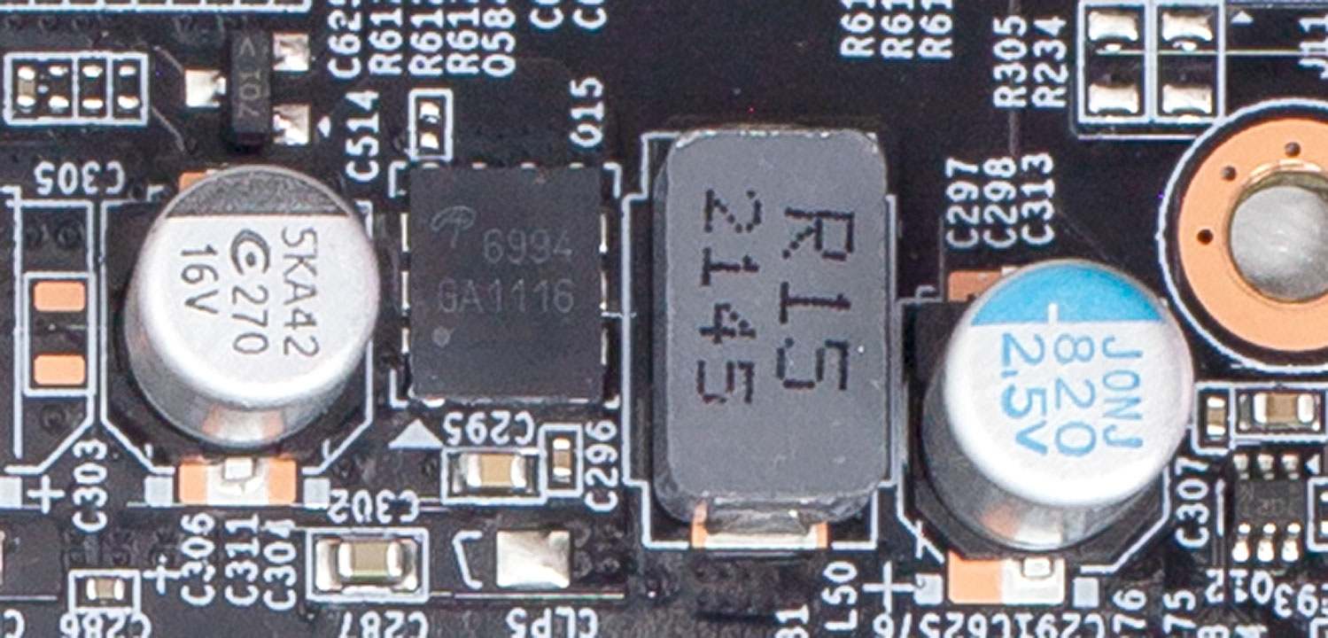
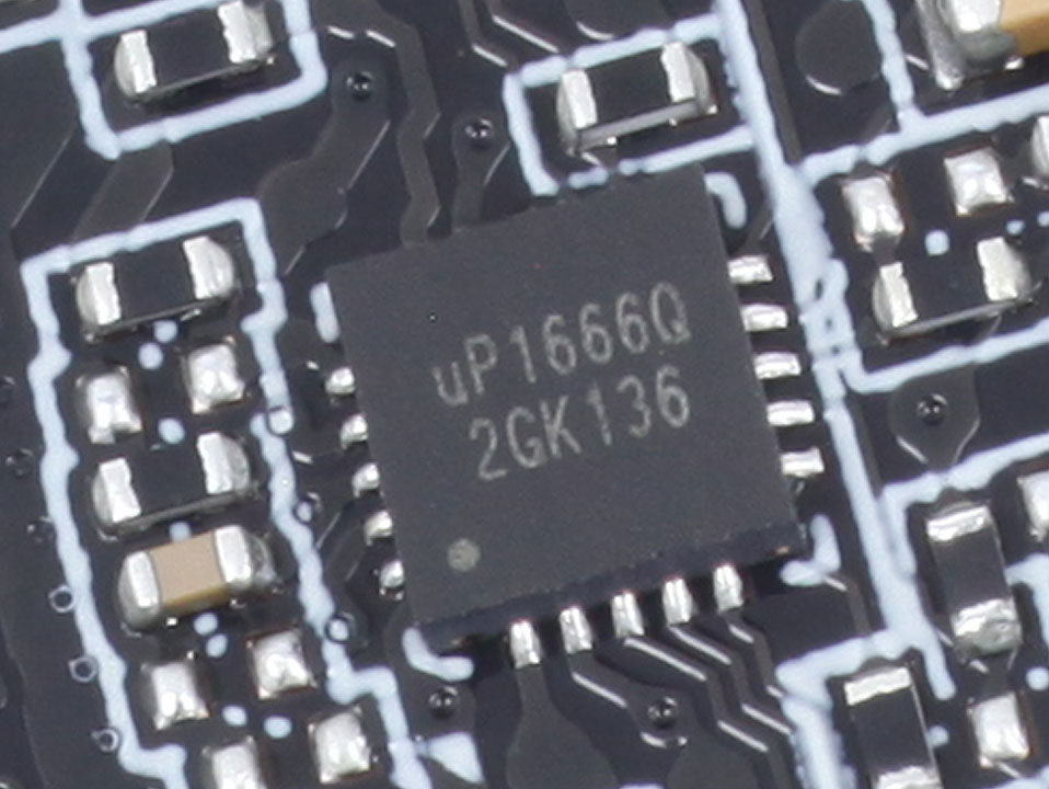
The memory VRM is single-phase and managed by a uPI uP1666Q controller.
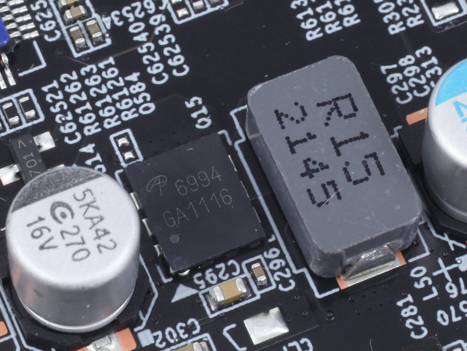
For memory, an Alpha Omega AON6994 dual-MOSFET is used. It's specified for currents up to 82 A.
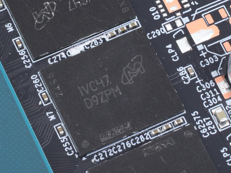
The GDDR6 memory chips are made by Micron and carry the model number D9ZPM, which decodes to MT61K512M32KPA-14:C. They are specified to run at 1750 MHz (14 Gbps GDDR6 effective).

NVIDIA's GA106 graphics processor is made using Samsung's 8 nanometer node and has a transistor count of 12 billion with a die size of 276 mm².
Apr 29th, 2024 18:00 EDT
change timezone
Latest GPU Drivers
New Forum Posts
- i7-1355U (9)
- 7900 XTX Seriously lacking (12)
- Dialing in the overlock on my new 12600kf, matured silicon process showing great results... (34)
- Arctic MX-6 shelf life is just a couple months? (26)
- What's your latest tech purchase? (20394)
- EK seems to be having major issues (56)
- Post your CrystalDiskMark speeds (598)
- Is it better for zero RPM PSUs to place the fan on top? (28)
- Looking for recommendations to upgrade the GPU (32)
- What are you playing? (20557)
Popular Reviews
- Ugreen NASync DXP4800 Plus Review
- HYTE THICC Q60 240 mm AIO Review
- Upcoming Hardware Launches 2023 (Updated Feb 2024)
- MOONDROP x Crinacle DUSK In-Ear Monitors Review - The Last 5%
- Team Group T-Force Vulcan ECO DDR5-6000 32 GB CL38 Review
- Thermalright Phantom Spirit 120 EVO Review
- AMD Ryzen 7 7800X3D Review - The Best Gaming CPU
- FiiO K19 Desktop DAC/Headphone Amplifier Review
- ASUS Radeon RX 7900 GRE TUF OC Review
- NVIDIA GeForce RTX 4090 PCI-Express Scaling
Controversial News Posts
- Windows 11 Now Officially Adware as Microsoft Embeds Ads in the Start Menu (152)
- Intel Statement on Stability Issues: "Motherboard Makers to Blame" (148)
- Sony PlayStation 5 Pro Specifications Confirmed, Console Arrives Before Holidays (117)
- NVIDIA Points Intel Raptor Lake CPU Users to Get Help from Intel Amid System Instability Issues (106)
- AMD's RDNA 4 GPUs Could Stick with 18 Gbps GDDR6 Memory (104)
- AMD "Strix Halo" Zen 5 Mobile Processor Pictured: Chiplet-based, Uses 256-bit LPDDR5X (103)
- US Government Wants Nuclear Plants to Offload AI Data Center Expansion (98)
- TechPowerUp Hiring: Reviewers Wanted for Motherboards, Laptops, Gaming Handhelds and Prebuilt Desktops (90)