 13
13
Gigabyte GeForce RTX 3090 Eagle OC Review
Test Setup »High-resolution PCB Pictures
These pictures are for the convenience of volt modders and people who would like to see all the finer details on the PCB. Feel free to link back to us and use these in your articles or forum posts.
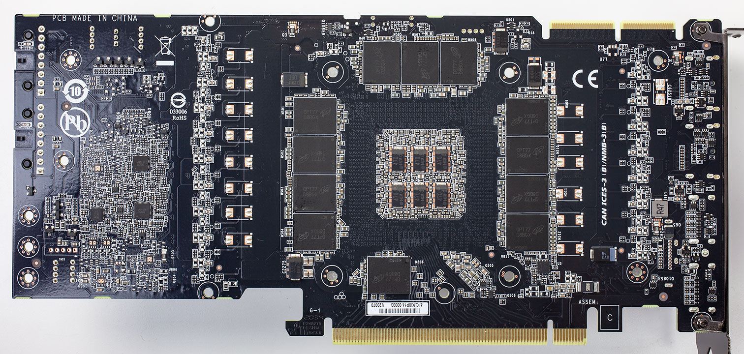
High-res versions are also available (front, back).
Circuit Board (PCB) Analysis


Unlike NVIDIA's Founders Edition boards, which implement MPS controllers, Gigabyte uses a trio of UPI 9512R controllers to manage the various power domains of the GA102 GPU.
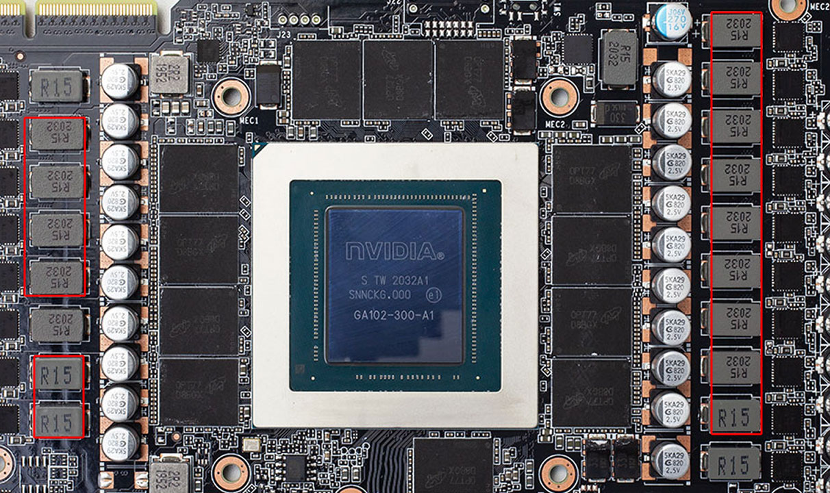
Together, the vGPU is a 15-phase setup.
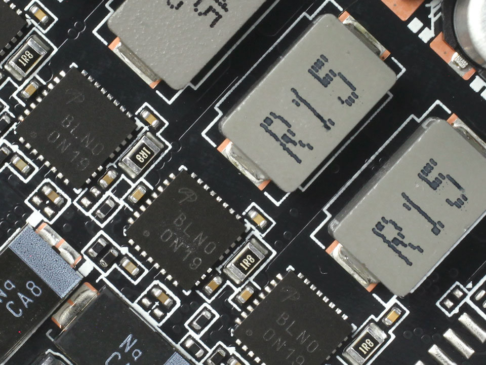
Gigabyte uses DrMOS components throughout.


Memory voltage uses a three-phase design and is generated by a UPI uS5650Q. Note the placement of the memory VRM phases—all spread out among the GPU power phases. The reason seems to be improved thermal performance and better voltage stability.

The GDDR6X memory chips are made by Micron and carry the model number D8BGX, which decodes to MT61K256M32JE-21. They are specified to run at 1313 MHz (21 Gbps GDDR6X effective).
GDDR6X doubles the data rate once again over GDDR6. It no longer transmits one bit of information by setting the voltage to either "on" or "off", but instead sends two bits of information at the same time by using four different voltage levels.

NVIDIA's GA102 graphics processor is the company's second Ampere architecture chip, the first one targeted at GeForce gamers. It is produced on a 8 nanometer process at Samsung and has a transistor count of 28 billion with a die size of 628 mm².
Apr 18th, 2024 00:06 EDT
change timezone
Latest GPU Drivers
New Forum Posts
- AMD RX 7000 series GPU Owners' Club (1063)
- 4K Gamers, How much VRAM do you have? (131)
- Your PC ATM (34483)
- Free Games Thread (3765)
- DDR5 RAM Speeds and the future (24)
- FINAL FANTASY XIV: Dawntrail Official Benchmark (46)
- EDP other basically constantly red while playing games (0)
- Will a RTX 4070 TI super bottleneck a Ryzen 9 7950X3D? (27)
- Looking for a great value 1080p gaming display (27)
- Gigabyte gpu model differences? (27)
Popular Reviews
- Horizon Forbidden West Performance Benchmark Review - 30 GPUs Tested
- PowerColor Radeon RX 7900 GRE Hellhound Review
- ASUS GeForce RTX 4090 Matrix Platinum Review - The RTX 4090 Ti
- Fractal Design Terra Review
- Corsair 2000D Airflow Review
- Minisforum EliteMini UM780 XTX (AMD Ryzen 7 7840HS) Review
- Creative Pebble X Plus Review
- FiiO KB3 HiFi Mechanical Keyboard Review - Integrated DAC/Amp!
- ASUS GeForce RTX 4090 STRIX OC Review
- NVIDIA GeForce RTX 4090 Founders Edition Review - Impressive Performance
Controversial News Posts
- Sony PlayStation 5 Pro Specifications Confirmed, Console Arrives Before Holidays (105)
- NVIDIA Points Intel Raptor Lake CPU Users to Get Help from Intel Amid System Instability Issues (102)
- US Government Wants Nuclear Plants to Offload AI Data Center Expansion (98)
- Windows 10 Security Updates to Cost $61 After 2025, $427 by 2028 (82)
- Developers of Outpost Infinity Siege Recommend Underclocking i9-13900K and i9-14900K for Stability on Machines with RTX 4090 (82)
- TechPowerUp Hiring: Reviewers Wanted for Motherboards, Laptops, Gaming Handhelds and Prebuilt Desktops (70)
- Intel Realizes the Only Way to Save x86 is to Democratize it, Reopens x86 IP Licensing (70)
- AMD Zen 5 Execution Engine Leaked, Features True 512-bit FPU (63)