 24
24
HIS Radeon HD 6950 2 GB Review
(24 Comments) »HD 6950 Review Introduction
It's finally here! AMD rolled out its latest high-end GPU, codenamed "Cayman", which tops the Northern Islands, AMD's second-generation DirectX 11 compliant GPU family. Using this, AMD is initially carving out two enthusiast-grade products: the AMD Radeon HD 6970 (reviewed here), and the Radeon HD 6950, both released today. There's also scope for a dual-GPU product in the near future. AMD's Cayman GPU faced quite a few hiccups en route today's launch. It was slated for mid-November, but was delayed by a month due to component shortage. Meanwhile, NVIDIA went ahead with a hard-launch of its GeForce GTX 580 graphics processor, and subsequently, the GeForce GTX 570.
With Cayman, AMD is introducing its biggest design change for the GPU's SIMD processing area since Radeon HD 2900 series, it's also introducing a greater amount of parallelism to the graphics engine, and doubling the standard memory amount from 1 GB in the previous generation Radeon HD 5870 and Radeon HD 5850, to 2 GB on both HD 6970 and HD 6950. As a brief lesson on AMD's naming scheme with this generation, Radeon HD 6950 and HD 6970 represent high-end single GPU SKUs, successors to HD 5800 series, while the recently introduced HD 6800 series are in a segment of their own with no definitive predecessors.
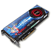
The Radeon HD 6970 from HIS we're reviewing today, sticks to AMD's reference board design, including adherence to reference clock speeds. With HD 6900 series, AMD made sure that users of all HD 6900, including those which are factory-overclocked, have access to reference clock speeds at the turn of a switch (detailed later down the review). It features 2 GB of GDDR5 memory, carries clock speeds of 880 MHz core and 1375 MHz (5500 MHz GDDR5 effective); and display outputs including two DVI, one HDMI 1.4a, and two mini DisplayPort 1.2.
Product Positioning
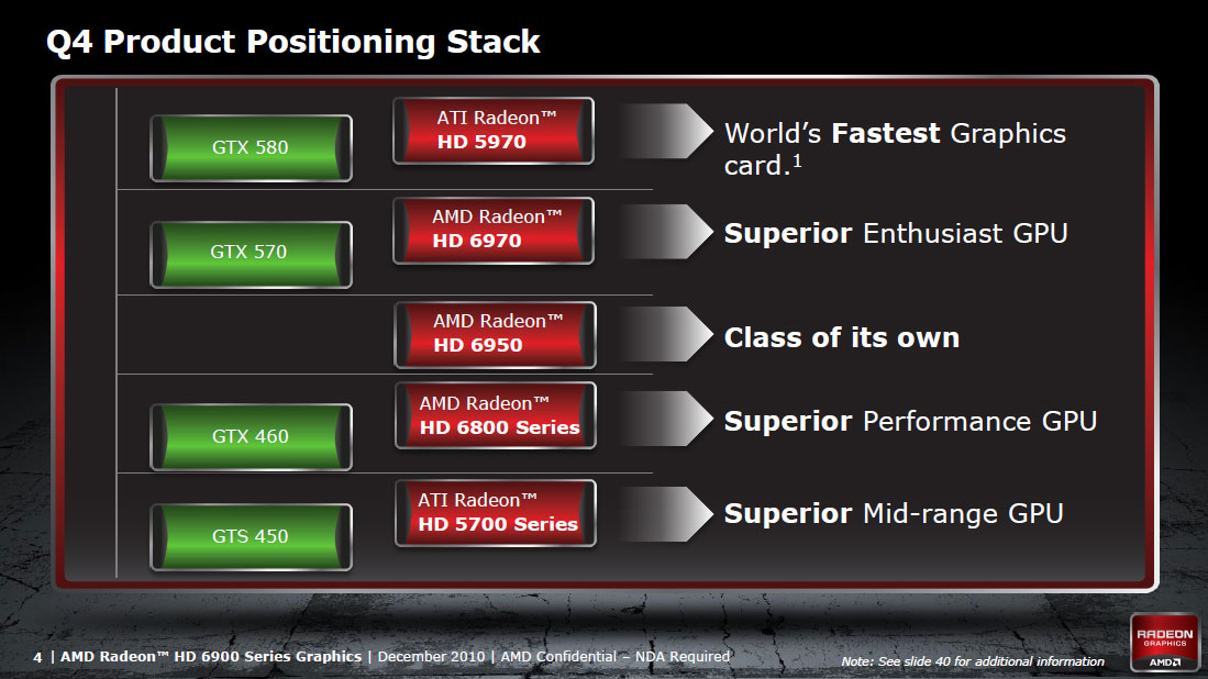
This slide from AMD instantly tells you the amount of damage the surprise hard-launch of NVIDIA GeForce 580 and GTX 570 caused. Take those two out of the equation, and we're actually seeing the GTX 480 (which has roughly the same performance as GTX 570) being edged past by HD 6970, and HD 6950 way ahead of whatever else is down there from NVIDIA (GTX 470, GTX 460 1 GB).AMD is still banking on the previous-generation HD 5970 dual-GPU graphics card to hold the performance leadership (which it is loosely holding on to, with the potential of losing it to the GTX 580 with one good GeForce driver snatching that leadership); HD 6970 to be a notch lower in price but somewhere between GTX 570 and GTX 580 in terms of performance.
| Radeon HD 6850 | Radeon HD 5850 | GeForce GTX 470 | Radeon HD 6870 | Radeon HD 5870 | Radeon HD 6950 | GeForce GTX 570 | GeForce GTX 480 | Radeon HD 6970 | GeForce GTX 580 | Radeon HD 5970 | |
| Shader units | 960 | 1440 | 448 | 1120 | 1600 | 1408 | 480 | 480 | 1536 | 512 | 2x 1600 |
| ROPs | 32 | 32 | 40 | 32 | 32 | 32 | 40 | 48 | 32 | 48 | 2x 32 |
| GPU | Barts | Cypress | GF100 | Barts | Cypress | Cayman | GF110 | GF100 | Cayman | GF110 | 2x Cypress |
| Transistors | 1700M | 2154M | 3200M | 1700M | 2154M | 2640M | 3000M | 3200M | 2640M | 3000M | 2x 2154M |
| Memory Size | 1024 MB | 1024 MB | 1280 MB | 1024 MB | 1024 MB | 2048 MB | 1280 MB | 1536 MB | 2048 MB | 1536 MB | 2x 1024 MB |
| Memory Bus Width | 256 bit | 256 bit | 320 bit | 256 bit | 256 bit | 256 bit | 320 bit | 384 bit | 256 bit | 384 bit | 2x 256 bit |
| Core Clock | 775 MHz | 725 MHz | 607 MHz | 900 MHz | 850 MHz | 800 MHz | 732 MHz | 700 MHz | 880 MHz | 772 MHz | 725 MHz |
| Memory Clock | 1000 MHz | 1000 MHz | 837 MHz | 1050 MHz | 1200 MHz | 1250 MHz | 950 MHz | 924 MHz | 1375 MHz | 1002 MHz | 1000 MHz |
| Price | $180 | $260 | $260 | $240 | $360 | $300 | $330 | $450 | $370 | $500 | $580 |
Architecture

Cayman, named after the lovely Cayman islands in the Caribbean, is AMD's new high-end GPU. It succeeds Cypress, on which were based Radeon HD 5800 series and the dual-GPU HD 5970. Cayman is built on existing 40 nm process at TSMC. Apart from the processor most of the components inside are the same as the ones found in the previous generation GPUs, except that the hierarchy of components is changed to add a degree of parallelism that goes a step ahead of even Barts. The SIMD cores are completely restructured, too.

With Cypress, there was only one graphics engine (that which computes preliminary data and instructions, and passes them on for low-level processing to the SIMD cores), and one dispatch processor that funneled data and instructions down to the two SIMD engine blocks. Barts introduced a degree of parallelism by giving each SIMD engine block its own dispatch processor, instruction and constant caches. Cayman is taking that a step further, by splitting even the graphics engines between the two SIMD engine blocks. This gives dedicated rasterizers, geometry assemblers to each block, but more importantly, doubles the number of tessellation units, with each graphics engine having one.


As mentioned earlier, AMD brought about a radical change in the stream processor design. Compared to the older VLIW5 design in which an SIMD core consisted of four simple and one complex stream processors with some common resources, the new design, dubbed VLIW4, combines four equally-capable complex stream processors, with two of the four getting special functions. Overall, with a stream processor count of 1536, the Radeon HD 6970 clocked at 880 MHz, is able to churn out a single-precision floating point (IEEE754-SP) performance of 2.7 TFLOPs, and double-precision performance (IEEE754-DP) of 675 GFLOPs. The VLIW4 architecture, hence is aimed to increase performance per mm² of die-area. The render back-ends, have also been redesigned to facilitate 2 times faster 16-bit integer and 32-bit floating-point operations.
In a nutshell, the Cayman die measures 389 mm², holding 2.64 billion transistors. It is built on the 40 nm TSMC process. It has 24 SIMD engines spread across two SIMD engine blocks. There are 1536 stream processors in all. There are 96 texture memory units (TMUs), and 32 raster operation processors (ROPs). New, faster memory controllers allow use of new 5.5 Gbps memory chips. The memory bus width is 256-bit, with which the GPU connects to eight 2 Gbit memory chips to archive 2 GB of total memory.
Packaging
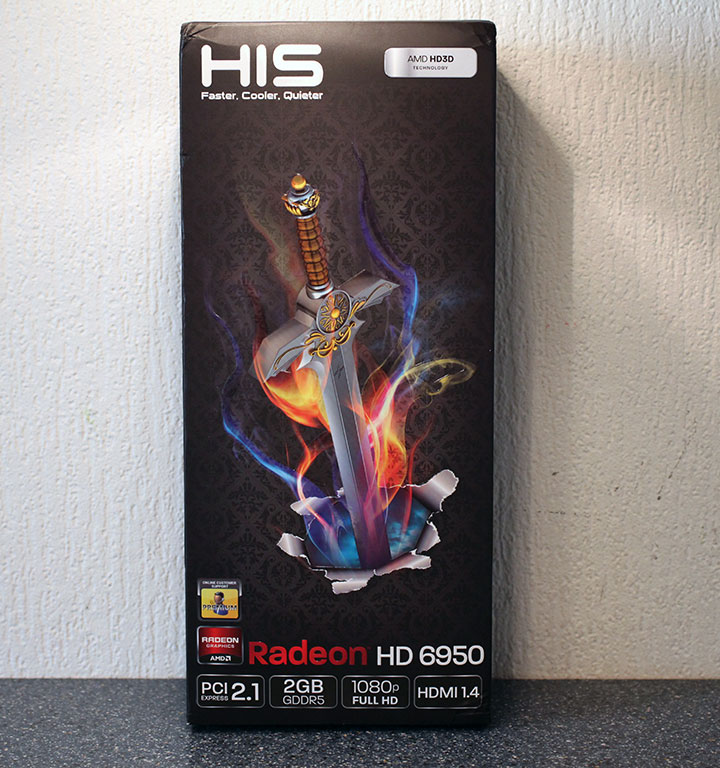
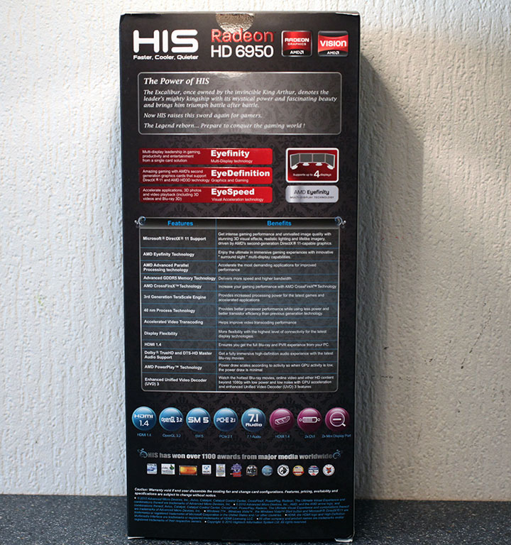
HIS uses their standard package design for the Radeon HD 6970.
Our Patreon Silver Supporters can read articles in single-page format.
Apr 26th, 2024 04:59 EDT
change timezone
Latest GPU Drivers
New Forum Posts
- Horizontal black lines popping up on my screen? (7)
- What's your latest tech purchase? (20343)
- TPU's Nostalgic Hardware Club (18471)
- What are you playing? (20531)
- Which new games will you be buying? (320)
- Alphacool CORE 1 CPU block - bulging with danger of splitting? (21)
- Best SSD for system drive (82)
- What phone you use as your daily driver? And, a discussion of them. (1484)
- AMD RX 7000 series GPU Owners' Club (1087)
- im new to throttelstop and i think i messed it up by copying others any hints would be very much aprreciated (3)
Popular Reviews
- Fractal Design Terra Review
- Thermalright Phantom Spirit 120 EVO Review
- Corsair 2000D Airflow Review
- ASUS GeForce RTX 4090 STRIX OC Review
- NVIDIA GeForce RTX 4090 Founders Edition Review - Impressive Performance
- ASUS GeForce RTX 4090 Matrix Platinum Review - The RTX 4090 Ti
- MSI GeForce RTX 4090 Suprim X Review
- Gigabyte GeForce RTX 4090 Gaming OC Review
- MSI GeForce RTX 4090 Gaming X Trio Review
- MSI GeForce RTX 4090 Suprim Liquid X Review
Controversial News Posts
- Windows 11 Now Officially Adware as Microsoft Embeds Ads in the Start Menu (121)
- Sony PlayStation 5 Pro Specifications Confirmed, Console Arrives Before Holidays (117)
- NVIDIA Points Intel Raptor Lake CPU Users to Get Help from Intel Amid System Instability Issues (106)
- AMD "Strix Halo" Zen 5 Mobile Processor Pictured: Chiplet-based, Uses 256-bit LPDDR5X (101)
- US Government Wants Nuclear Plants to Offload AI Data Center Expansion (98)
- AMD's RDNA 4 GPUs Could Stick with 18 Gbps GDDR6 Memory (89)
- Developers of Outpost Infinity Siege Recommend Underclocking i9-13900K and i9-14900K for Stability on Machines with RTX 4090 (85)
- Windows 10 Security Updates to Cost $61 After 2025, $427 by 2028 (84)