 22
Intel Arc A750 Review - Great Value
(22 Comments) »Introduction

Intel's Arc 7-series is finally here, with the promise of high performance gaming at competitive prices. The new Arc A750 "Alchemist" launches at just $289, and we have the review for you. Intel's new card promises AAA gaming at 1080p and 1440p resolutions, or high refresh-rate e-sports gaming. The company's entry to the gaming discrete graphics space is mainly a byproduct of the company's investments in the highly scalable Xe HPC/AI compute processors, to grab a slice of this high-margin pie. While NVIDIA and AMD scaled up their traditional GPUs and stripped them of graphics-rendering hardware to create their compute processors; Intel's development is in the opposite direction—to scale down its compute processors and add graphics-relevant hardware. Since Intel has a reputation for being perfectionists with silicon engineering, and that they're known not to enter a market unless they can make the best processors; the new Xe-HPG graphics architecture enters the market in the performance-segment. The Arc 7-series will compete with the best selling SKUs of both NVIDIA and AMD—the GeForce RTX 3060 and Radeon RX 6600 XT. If Intel can crack this market, we might get a third player in the GPU market, which will lead to more competition at better prices.

The Arc A750 is based on the same 6 nm ACM-G10 silicon as the $349 A770 Limited Edition which we're also reviewing today, but is slightly cut down. While the A770 maxes the silicon out with all 32 Xe Cores across 8 Render Slices, the A750 is carved out by disabling one of those Render Slices, leaving us with 7, or 28 Xe Cores. The memory size is set at 8 GB, across the same 256-bit GDDR6 memory bus width; but at a slower data-rate of 16 Gbps (512 GB/s total bandwidth), compared to 17.5 Gbps (560 GB/s bandwidth) of the A770. There's no 16 GB variant, unlike with the A770.
The Arc A750 targets the same class of gamers as the A770—1080p or 1440p AAA gaming at high to extreme settings; with real-time ray tracing added to the mix. You can enable XeSS and yield higher performance at minimal quality loss, much like you can with DLSS on NVIDIA, and FSR on AMD. Much like FSR, XeSS works on all brands of GPUs, however, on Arc GPUs, XeSS takes advantage of the Intel XMX matrix-acceleration, offering a much higher performance uplift. Intel also claims technological parity with NVIDIA for its ray tracing architecture, where Arc GPUS rely as extensively on fixed-function hardware as NVIDIA GPUs do. The shader reordering technology used by Intel is on-par with what NVIDIA is only now beginning to roll out with its RTX 40-series "Ada" architecture.
Intel Arc graphics family has full support for the DirectX 12 Ultimate software feature-set, including real time ray tracing, variable rate shading, mesh shaders, and sampler feedback. It also supports other APIs, such as Vulkan and OpenGL. Some older versions of Direct3D, such as D3D9, are emulated on D3D12. In this review, we take the Arc A750 for a test-drive along our vast selection of games, to show you if it's better value for money than the A770.
| Price | Cores | ROPs | Core Clock | Boost Clock | Memory Clock | GPU | Transistors | Memory | |
|---|---|---|---|---|---|---|---|---|---|
| RX 5600 XT | $210 | 2304 | 64 | 1375 MHz | 1560 MHz | 1500 MHz | Navi 10 | 10300M | 6 GB, GDDR6, 192-bit |
| RX 6500 XT | $170 | 1024 | 32 | 2685 MHz | 2825 MHz | 2248 MHz | Navi 24 | 5400M | 4 GB, GDDR6, 64-bit |
| RTX 2060 | $240 | 1920 | 48 | 1365 MHz | 1680 MHz | 1750 MHz | TU106 | 10800M | 6 GB, GDDR6, 192-bit |
| RX Vega 64 | $320 | 4096 | 64 | 1247 MHz | 1546 MHz | 953 MHz | Vega 10 | 12500M | 8 GB, HBM2, 2048-bit |
| RX 5700 XT | $300 | 2560 | 64 | 1605 MHz | 1755 MHz | 1750 MHz | Navi 10 | 10300M | 8 GB, GDDR6, 256-bit |
| RTX 3050 | $290 | 2560 | 32 | 1552 MHz | 1777 MHz | 1750 MHz | GA106 | 12000M | 8 GB, GDDR6, 128-bit |
| RTX 2070 | $300 | 2304 | 64 | 1410 MHz | 1620 MHz | 1750 MHz | TU106 | 10800M | 8 GB, GDDR6, 256-bit |
| RX 6600 | $250 | 1792 | 64 | 2044 MHz | 2491 MHz | 1750 MHz | Navi 23 | 11060M | 8 GB, GDDR6, 128-bit |
| RTX 3060 | $370 | 3584 | 48 | 1320 MHz | 1777 MHz | 1875 MHz | GA106 | 12000M | 12 GB, GDDR6, 192-bit |
| RX 6600 XT | $300 | 2048 | 64 | 2359 MHz | 2589 MHz | 2000 MHz | Navi 23 | 11060M | 8 GB, GDDR6, 128-bit |
| RX 6650 XT | $300 | 2048 | 64 | 2410 MHz | 2635 MHz | 2190 MHz | Navi 23 | 11060M | 8 GB, GDDR6, 128-bit |
| Arc A750 | $290 | 3584 | 112 | 2050 MHz | N/A | 2000 MHz | ACM-G10 | 21700M | 8 GB, GDDR6, 256-bit |
| Arc A770 | $350 | 4096 | 128 | 2100 MHz | N/A | 2187 MHz | ACM-G10 | 21700M | 16 GB, GDDR6, 256-bit |
| RTX 2080 | $400 | 2944 | 64 | 1515 MHz | 1710 MHz | 1750 MHz | TU104 | 13600M | 8 GB, GDDR6, 256-bit |
| RTX 3060 Ti | $450 | 4864 | 80 | 1410 MHz | 1665 MHz | 1750 MHz | GA104 | 17400M | 8 GB, GDDR6, 256-bit |
| RX 6700 XT | $410 | 2560 | 64 | 2424 MHz | 2581 MHz | 2000 MHz | Navi 22 | 17200M | 12 GB, GDDR6, 192-bit |
| RX 6750 XT | $470 | 2560 | 64 | 2495 MHz | 2600 MHz | 2250 MHz | Navi 22 | 17200M | 12 GB, GDDR6, 192-bit |
| RTX 2080 Ti | $550 | 4352 | 88 | 1350 MHz | 1545 MHz | 1750 MHz | TU102 | 18600M | 11 GB, GDDR6, 352-bit |
| RTX 3070 | $530 | 5888 | 96 | 1500 MHz | 1725 MHz | 1750 MHz | GA104 | 17400M | 8 GB, GDDR6, 256-bit |
| RTX 3070 Ti | $600 | 6144 | 96 | 1575 MHz | 1770 MHz | 1188 MHz | GA104 | 17400M | 8 GB, GDDR6X, 256-bit |
| RX 6800 | $580 | 3840 | 96 | 1815 MHz | 2105 MHz | 2000 MHz | Navi 21 | 26800M | 16 GB, GDDR6, 256-bit |
Architecture


Intel Xe-HPG "Alchemist" graphics architecture sees its biggest implementation to date with the ACM-G10 silicon powering the A770 and A750. Built on the 6 nm process at TSMC, the ACM-G10 measures 406 mm² in die-area, and packs 21.7 billion transistors. Much like NVIDIA and AMD, Intel has innovated its own hierarchy for the number-crunching machinery of its GPUs, and differentiates SKUs by changing the number of indivisible groups of these to meet performance targets. The ACM-G10 silicon features a PCI-Express 4.0 x16 host interface, a 256-bit wide GDDR6 memory interface, the Xe Media Engine and Xe Display Engine, among a global dispatch processor, and memory fabric that's cushioned by L2 cache. The main SIMD component top-level organization is the Render Slice. Each of these is a self-contained unit with all the number-crunching and raster graphics hardware a GPU needs.


The ACM-G10 features eight such Render Slices. Each of these features four blocks of indivisible processing machinery, called Xe Cores; four Ray Tracing Units (RT units), and DirectX 12 Ultimate optimized raster-graphics units that includes four Samplers, Tessellation geometry processors, 16 ROPs, and 32 TMUs. Since there are 8 Render Slices, the silicon physically has 16 RT units, 128 ROPs, and 256 TMUs.
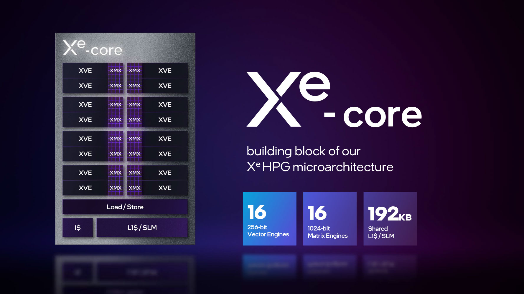

The Xe Core is the indivisible computation core, with sixteen 256-bit Vector Engines (execution units), sixteen 1024-bit XMX Matrix Engines, and 192 KB of L1 cache. Each Vector Engine has eight each of FP and INT units, besides a register file. Two adjacent Vector Engines share a Thread Control unit to share execution waves. There are 16 VEs per Xe Core, 4 Xe Cores per Render Slice, and 8 Render Slices on the ACM-G10 silicon, so we have 512 execution units in all, each with 8 FP/INT execution stages, which logically work out to 4,096 unified shaders. The Arc A770 is configured with all 32 Xe Cores, so it gets 4,096 shaders. The A750 gets 28 Xe Cores, or 7 out of 8 Render Slices, or 448 execution units, amounting to 3,584 unified shaders.
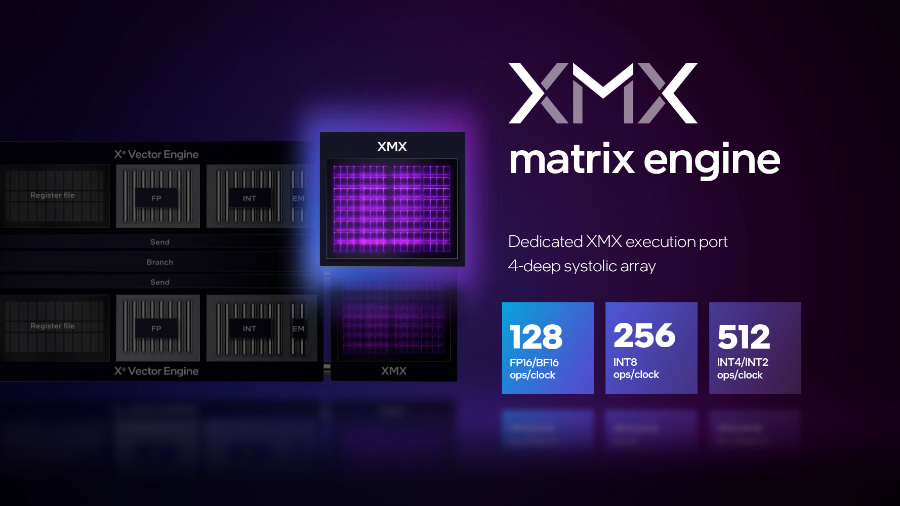
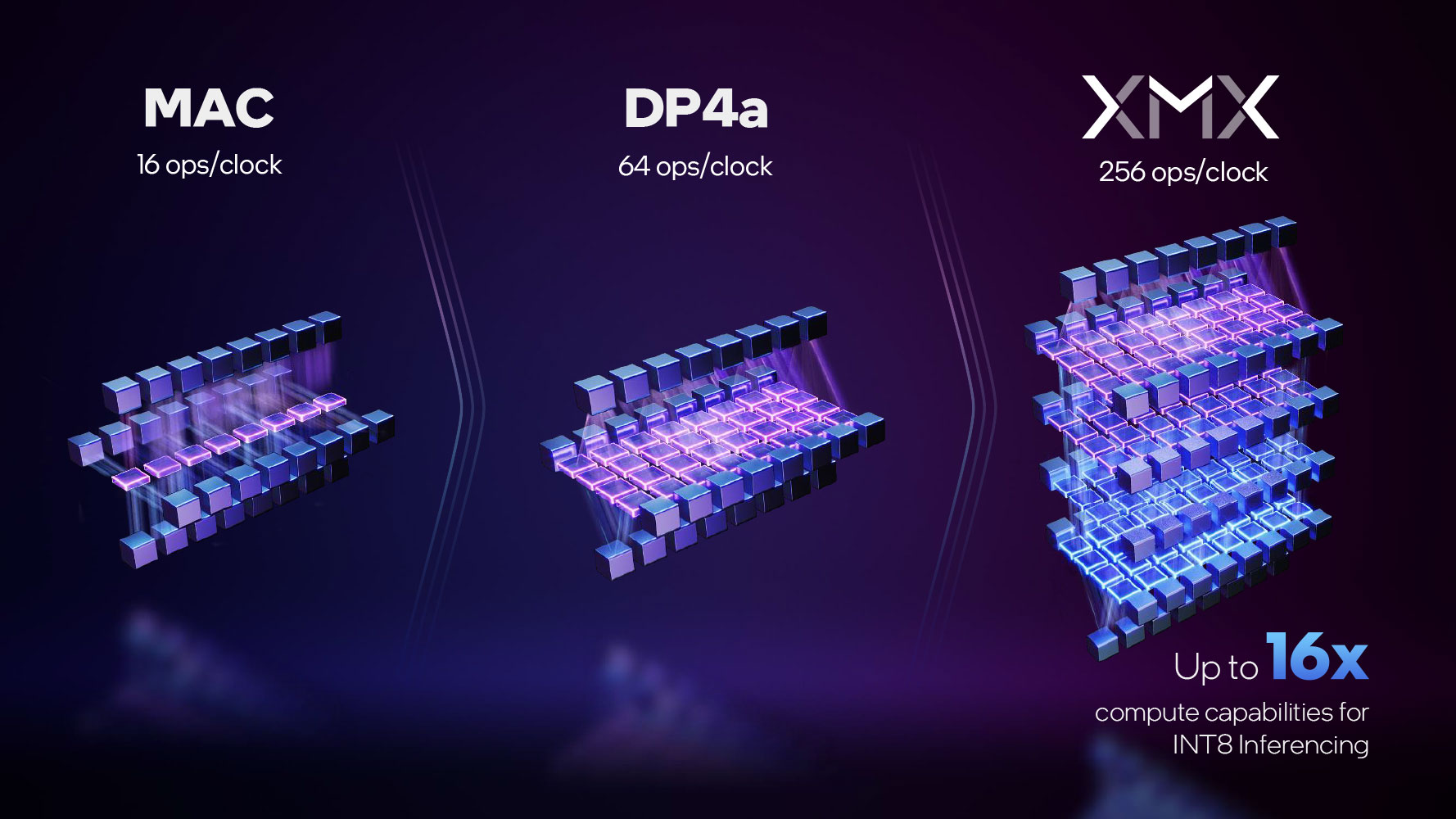
The XMX Matrix Engine is an extremely capable matrix-multiplication fixed-function hardware that can accelerate AI deep-learning neural net building and training. It's also a highly capable math accelerator. Intel originally designed this technology for the Xe-HP AI processors, but it finds client applications in Arc Graphics, where it is leveraged for ray tracing denoising and to accelerate features such as XeSS. There are 16 XMX units per Xe Core, and 64 per Render Slice, 512 across the ACM-G10 silicon. Each XMX unit can handle 128 FP16 or BF16 operations per clock; up to 256 INT8 ops/clock, and 512 INT4 ops/clock. The XMX-optimized native XeSS code is an order of magnitude faster than the industry-standard DP4a codepath of XeSS, as you'll see in our testing.

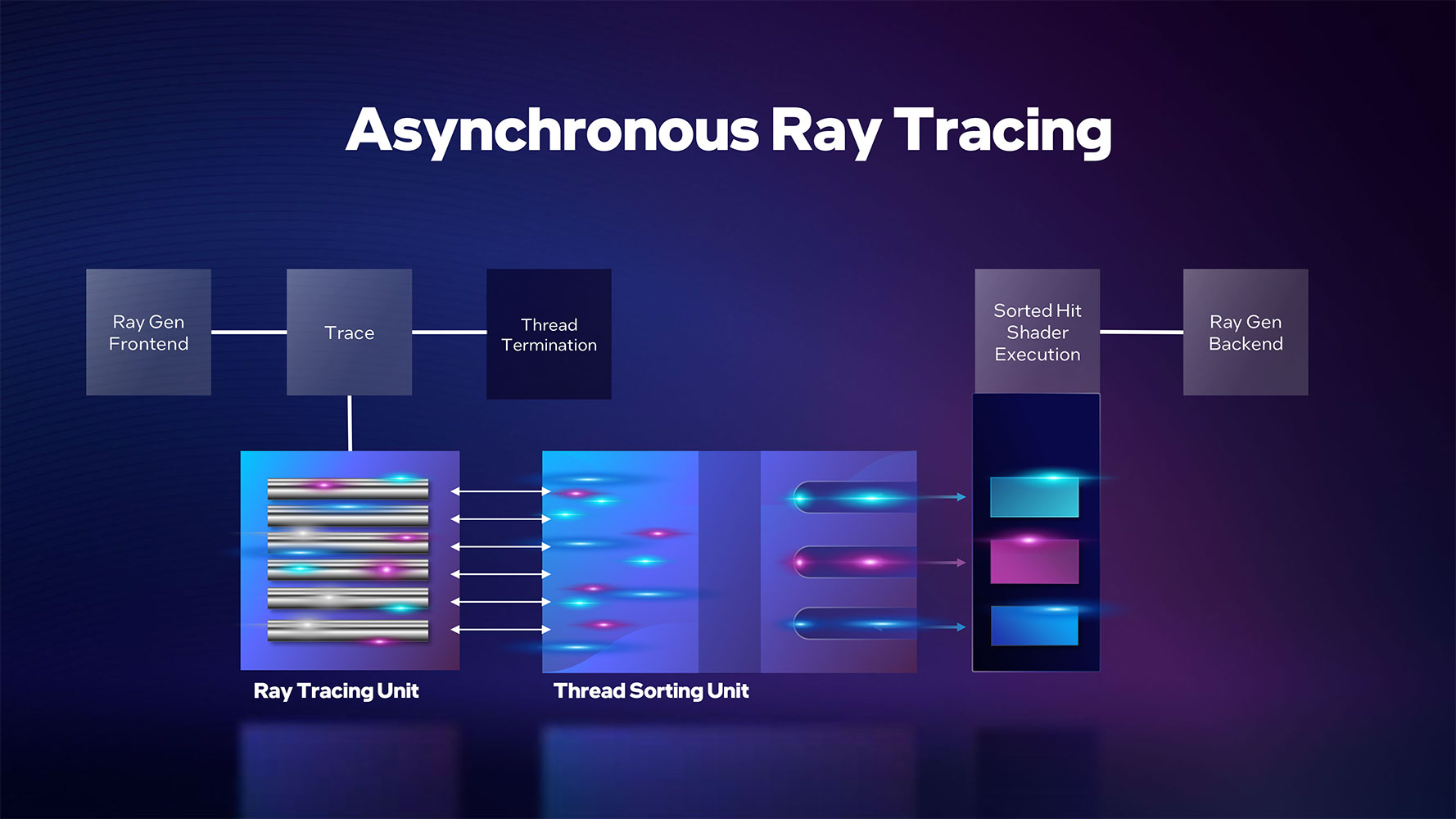
When it comes to real time ray tracing, Intel's Xe-HPG architecture has technological-parity with NVIDIA RTX, due to its heavy reliance on fixed-function hardware for ray intersection, BVH, and AI-based denoising.


There are several optimizations that further reduce the burden of ray tracing operations on the main SIMD machinery, such as shader execution reordering which optimizes shader work threads for streamlined execution among the SIMD units. NVIDIA is only now implementing such a feature, with its GeForce "Ada" architecture. There's a special component in each Xe Core that reorders shader threads. It's essentially a very intelligent dispatch unit. Intel refers to its ray tracing architecture as Asynchronous.


With Moore's Law tapering despite Intel claiming otherwise, the writing is on the wall—rendering at native resolution is over, at least in the performance and mainstream GPU segments. High-quality super resolution features such as DLSS and FSR are helping NVIDIA and AMD shore up performance at minimal quality loss, by rendering games at lower resolutions than native to the display; and upscaling them intelligently, with minimal quality losses. Intel's take is XeSS. The company claims that this is a 2nd generation super-res technology, on par with DLSS 2 and FSR 2.0. The XeSS upscaling tech is as easily integrated with a game engine's rendering pipeline as TAA (or AMD FSR). The XeSS algorithm is executed as XMX-optimized AI on Arc GPUs, and as DP4a-compatible code on other GPU brands. The algorithm takes into account low-resolution frame data, motion vectors, and temporal data from previously output high-res frames to reconstruct details, before passing on the high-res output to the game engine for post-processing and UI/HUD.
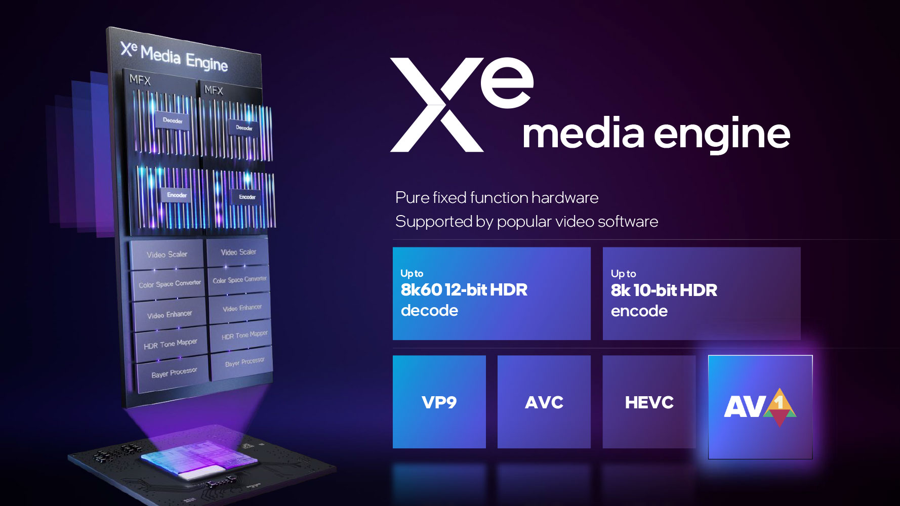

The Xe Display Engine is capable of up to two display outputs at 8K 60 Hz + HDR; up to four outputs at 4K 120 Hz + HDR, and up to four 1440p or 1080p with 360 Hz + HDR. VESA Adaptive Sync and Intel Smooth Sync features are supported. The latter is a feature that runs the GPU at its native frame-rate, while attempting to remove the screen-tearing from the display output. A typical Arc desktop graphics card has two each of DisplayPort 2.0 and HDMI 2.0b connections. The Xe Media Engine provides hardware-accelerated decoding and encoding of AV1, and accelerated decoding of H.265 HEVC, and H.264 AVC.
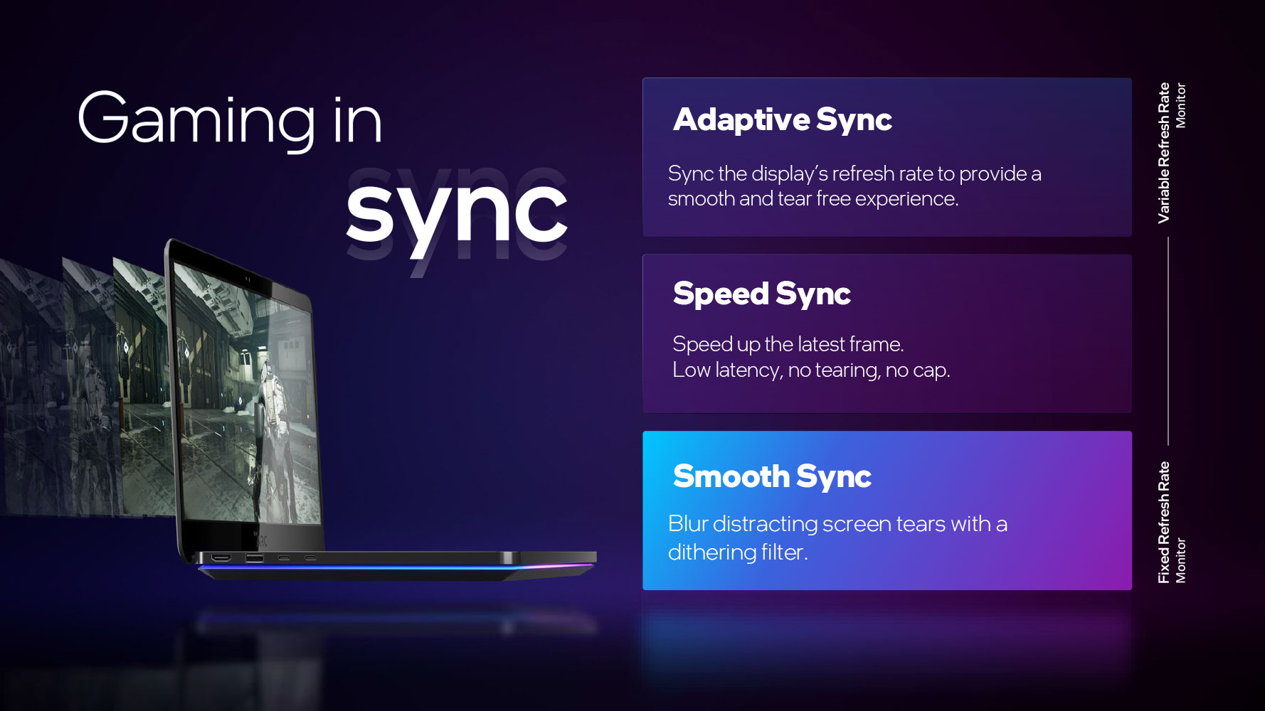
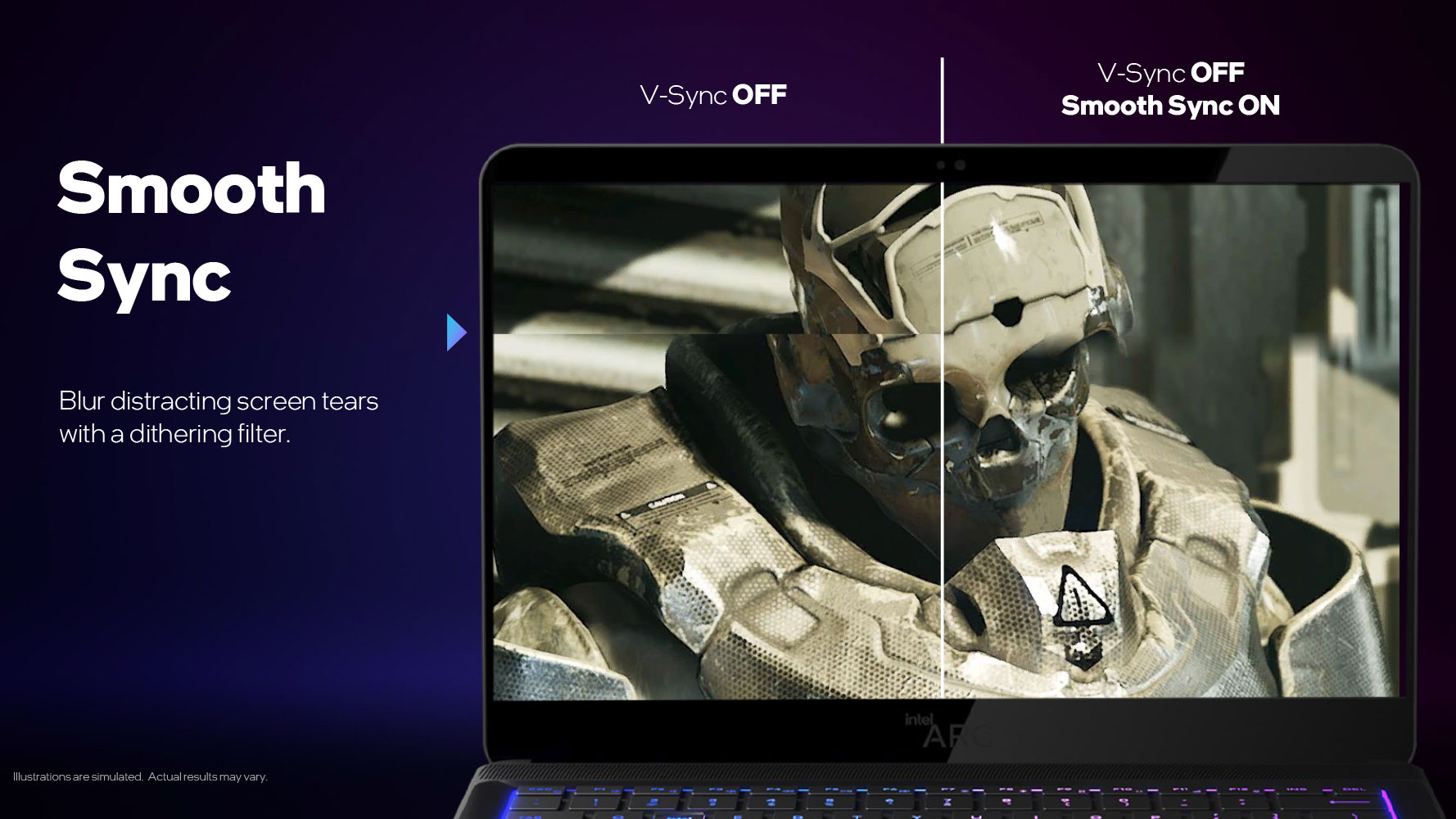
Besides VESA Adaptive Sync, the Xe Display Engine offers a software feature called Smooth Sync. This gives fixed refresh-rate monitors the ability to play games without V-Sync, rendering them at the highest possible FPS (and the least input latency), while attempting to eliminate the screen-tearing using a shader-based dithering filter pass. This is an extremely simply way to solve this problem, and we're surprised AMD and NVIDIA haven't tried it.
Packaging


The Card


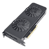
The Intel Arc A750 graphics card looks stunning, thanks to a clean design language that reminds of what Apple is offering with their iPhones. Visually, there's almost no difference between Arc A770 and Arc A750, except for the printed name of course. The only difference is that the A770 has a small RGB connector near its power inputs, the A750 does not have any RGB lighting.


Dimensions of the card are 27.0 x 11.5 cm, and it weighs 1087 g.


Installation requires two slots in your system.

Display connectivity includes three standard DisplayPort 2.0 ports and one HDMI 2.1.

The card has one 8-pin and one 6-pin power input. This configuration is rated for up to 300 W of power draw. If you look closely, you'll notice that the connectors are slightly mismatched in color. We confirmed with Intel that this will be fixed on future production runs, but some cards will make it in the retail market.
Teardown

Taking the Arc A750 apart is slightly more complicated than cards from other brands. While there's solid engineering everywhere, I suspect that the limited experience Intel has with building such cards is why some things are solved in a slightly less efficient way.
First, you have to take off the "backplate", which is a thin metal plate that's glued to the frame on the back of the card. Yup, glue isn't good for enthusiast end-users, I would have preferred a design with screws, as that's much easier to maintain. If you heat up the backplate with a heat gun, the glue will get soft and easy to remove.


Once the backplate is removed there's a bunch of Torx screws to take out, nothing out of the ordinary. Here we've encountered some sort of cooling plate that sits on top of the VRMs on the back—except there are no VRMs on this side, just an empty silkscreen on the PCB.


Now you can separate the cooler from the PCB assembly.


This metal reinforcement brace covers the PCB and helps strengthen it against bending.


Intel's cooler uses a large vapor-chamber baseplate paired with five heatpipes.
High-resolution PCB Pictures
These pictures are for the convenience of volt modders and people who would like to see all the finer details on the PCB. Feel free to link back to us and use these in your articles, videos or forum posts.

High-resolution versions are also available (front, back).
Our Patreon Silver Supporters can read articles in single-page format.
Nov 21st, 2026 04:29 PST
change timezone
Latest GPU Drivers
New Forum Posts
- WarpCoreBench scores! (88)
- What's your latest tech Freebie? (86)
- TPU's Nostalgic Hardware Club (22179)
- [Poll] 12V-2x6 Connector Protection: What Are You Using? (WireView / Ampinel / Equalizer / Other / Nothing) (50)
- UPS what one to get? (1)
- Anthrophics IPO (28)
- RX 9000 series GPU Owners Club (2252)
- Windows 11 General Discussion (7743)
- Without Jensen, PC gaming will be (52)
- Zen 3 IF/IMC degradation (242)
Popular Reviews
- Microsoft Surface Laptop Ultra Review - The Next-gen Arm Laptop
- Ugreen NASync DXP4800 GT Review
- Corsair RM1200e (Second Generation) Review
- Pulsar Office Tour & First Look at P1 Dual-Sensor Mouse
- Upcoming Hardware Launches 2027 (Updated Nov 2026)
- Acemagic Retro X3 Review
- Biwin Black Opal NV7400 2 TB Review
- AMD Ryzen 7 9800X3D Review - The Best Gaming Processor
- AMD Zen 6 Technical Deep Dive
- Chieftec Iceberg PRO 360 DARK Review
TPU on YouTube
Controversial News Posts
- NVIDIA Co-Founder and CEO Jensen Huang Officially Resigns (491)
- Report: Jensen Huang Eyes NVIDIA Comeback (257)
- Open Letter Asking NVIDIA to Reinstate Jensen Huang Passes 115,000 Signatures (184)
- OpenAI CEO Argues Home PCs Waste the World's Limited DRAM Supply (152)
- NVIDIA Launches Investigation Into Jensen Huang's Relationship With Suspected Chinese Spy (136)
- Intel "Raptor Lake Next" 16-Core and 20-Core CPUs Surface (130)
- Legendary Game Studio BioWare Shuts Down Following EA Layoffs (104)
- NVIDIA GeForce RTX 50-Series Scheduled for up to $500 Price Hike This Week (89)