 105
105
Intel Core i3-12100F Review - 5.2 GHz OC with an Asterisk
(105 Comments) »Introduction
The Core i3-12100F is designed to be the entry-level processor for Intel's Alder Lake architecture. Priced at just $105, this 4-core/8-thread CPU has all the ingredients needed to make it the next value king.
While Intel introduced their "Gracemont" Efficiency cores (or E-cores) with the high-end Alder Lake processors, the lower end of the lineup doesn't get this new capability. Rather, the Core i3-12100F is very similar in its design to previous generations—it's a monolithic chip design with a single type of processing core. This of course avoids compatibility issues and ensures the Core i3-12100F in this review will run best on any OS, not just Windows 11.

There's another big difference between the Core i3-12100F compared to the Core i5/7/9 K-models. The newer chips are based on a physically different silicon, dubbed "H0." This die is smaller and physically only features six "Golden Cove" P-cores, zero "Gracemont" E-core clusters, and a shared L3 cache that's only 18 MB. The higher-end CPUs are carved out of the larger "C0" die, the same one the flagship i9-12900K is based on.
The I/O capabilities of the "H0" silicon appears unchanged from "C0;" it puts out 16 PCI-Express Gen 5 lanes for the PEG slot (the main x16 slot meant for your graphics card), four PCI-Express Gen 4 lanes for a CPU-attached M.2 NVMe slot, and an 8-lane DMI 4.0 chipset-bus. It supports both DDR5 and DDR4 memory types. As an "F" SKU, the reviewed Core i3-12100F lacks onboard graphics. It's hence targeted squarely at users with a discrete graphics card. It also lacks an unlocked base-clock multiplier, and Intel rated the chip's processor base power (PBP) at 58 W, with maximum turbo power (MTP) at 89 W. The processor has a nominal clock speed of 3.30 GHz, with a maximum turbo boost frequency of 4.30 GHz. There's no fancy Turbo Boost Max 3.0 (and hence no preferred cores being exposed to the OS), but you get classic Turbo Boost 2.0.
Intel is pricing the Core i3-12100F at $97 for resellers. We bought our review sample for €110, including 19% VAT, which converts to $105. In the States, supply seems to be scarce at the moment, so prices are a bit higher. If you absolutely want onboard graphics, you can pick its twin, the Core i3-12100 for around $140. We chose the i3-12100F for review because we wanted to test just how much processing muscle you get for close to $100, and whether it's all you need for gaming these days, so you could push the money saved toward graphics.
| Price | Cores / Threads | Base Clock | Max. Boost | L3 Cache | TDP | Architecture | Process | Socket | |
|---|---|---|---|---|---|---|---|---|---|
| Core i3-9100F | $145 | 4 / 4 | 3.6 GHz | 4.2 GHz | 6 MB | 65 W | Coffee Lake | 14 nm | LGA 1151 |
| Core i3-10100 | $130 | 4 / 8 | 3.6 GHz | 4.3 GHz | 6 MB | 65 W | Comet Lake | 14 nm | LGA 1200 |
| Core i3-12100F | $105 | 4 / 8 | 3.3 GHz | 4.3 GHz | 12 MB | 58 W | Alder Lake | 10 nm | LGA 1700 |
| Ryzen 3 3100 | $150 | 4 / 8 | 3.6 GHz | 3.9 GHz | 16 MB | 65 W | Zen 2 | 7 nm | AM4 |
| Ryzen 3 3300X | $240 | 4 / 8 | 3.8 GHz | 4.3 GHz | 16 MB | 65 W | Zen 2 | 7 nm | AM4 |
| Core i3-10300 | $175 | 4 / 8 | 3.7 GHz | 4.4 GHz | 8 MB | 65 W | Comet Lake | 14 nm | LGA 1200 |
| Core i3-12300 | $155 | 4 / 8 | 3.5 GHz | 4.4 GHz | 12 MB | 60 W | Alder Lake | 10 nm | LGA 1700 |
| Core i5-9400F | $170 | 6 / 6 | 2.9 GHz | 4.1 GHz | 9 MB | 65 W | Coffee Lake | 14 nm | LGA 1151 |
| Core i5-10400F | $180 | 6 / 12 | 2.9 GHz | 4.3 GHz | 12 MB | 65 W | Comet Lake | 14 nm | LGA 1200 |
| Core i5-11400F | $215 | 6 / 12 | 2.6 GHz | 4.4 GHz | 12 MB | 65 W | Rocket Lake | 14 nm | LGA 1200 |
| Core i5-12400F | $180 | 6 / 12 | 2.5 GHz | 4.4 GHz | 18 MB | 65 W | Alder Lake | 10 nm | LGA 1700 |
| Core i5-10500 | $225 | 6 / 12 | 3.1 GHz | 4.5 GHz | 12 MB | 65 W | Comet Lake | 14 nm | LGA 1200 |
| Ryzen 5 3600 | $230 | 6 / 12 | 3.6 GHz | 4.2 GHz | 32 MB | 65 W | Zen 2 | 7 nm | AM4 |
| Core i5-9600K | $210 | 6 / 6 | 3.7 GHz | 4.6 GHz | 9 MB | 95 W | Coffee Lake | 14 nm | LGA 1151 |
| Core i5-10600K | $260 | 6 / 12 | 4.1 GHz | 4.8 GHz | 12 MB | 125 W | Comet Lake | 14 nm | LGA 1200 |
| Core i5-11600K | $260 | 6 / 12 | 3.9 GHz | 4.9 GHz | 12 MB | 125 W | Rocket Lake | 14 nm | LGA 1200 |
| Ryzen 5 3600X | $290 | 6 / 12 | 3.8 GHz | 4.4 GHz | 32 MB | 95 W | Zen 2 | 7 nm | AM4 |
| Ryzen 5 5600G | $250 | 6 / 12 | 3.9 GHz | 4.4 GHz | 16 MB | 65 W | Zen 3 + Vega | 7 nm | AM4 |
| Ryzen 5 5600X | $310 | 6 / 12 | 3.7 GHz | 4.6 GHz | 32 MB | 65 W | Zen 3 | 7 nm | AM4 |
| Core i5-12600K | $300 | 6+4 / 16 | 3.7 / 2.8 GHz | 4.9 / 3.6 GHz | 20 MB | 125 W | Alder Lake | 10 nm | LGA 1700 |
| Core i7-9700K | $310 | 8 / 8 | 3.6 GHz | 4.9 GHz | 12 MB | 95 W | Coffee Lake | 14 nm | LGA 1151 |
| Core i7-10700K | $330 | 8 / 16 | 3.8 GHz | 5.1 GHz | 16 MB | 125 W | Comet Lake | 14 nm | LGA 1200 |
| Core i7-11700K | $350 | 8 / 16 | 3.6 GHz | 5.0 GHz | 16 MB | 125 W | Rocket Lake | 14 nm | LGA 1200 |
| Ryzen 7 3700X | $320 | 8 / 16 | 3.6 GHz | 4.4 GHz | 32 MB | 65 W | Zen 2 | 7 nm | AM4 |
| Ryzen 7 5700G | $350 | 8 / 16 | 3.8 GHz | 4.6 GHz | 16 MB | 65 W | Zen 3 + Vega | 7 nm | AM4 |
| Ryzen 7 3800XT | $400 | 8 / 16 | 3.9 GHz | 4.7 GHz | 32 MB | 105 W | Zen 2 | 7 nm | AM4 |
| Core i7-12700K | $420 | 8+4 / 20 | 3.6 / 2.7 GHz | 5.0 / 3.8 GHz | 25 MB | 125 W | Alder Lake | 10 nm | LGA 1700 |
| Ryzen 7 5800X | $400 | 8 / 16 | 3.8 GHz | 4.7 GHz | 32 MB | 105 W | Zen 3 | 7 nm | AM4 |

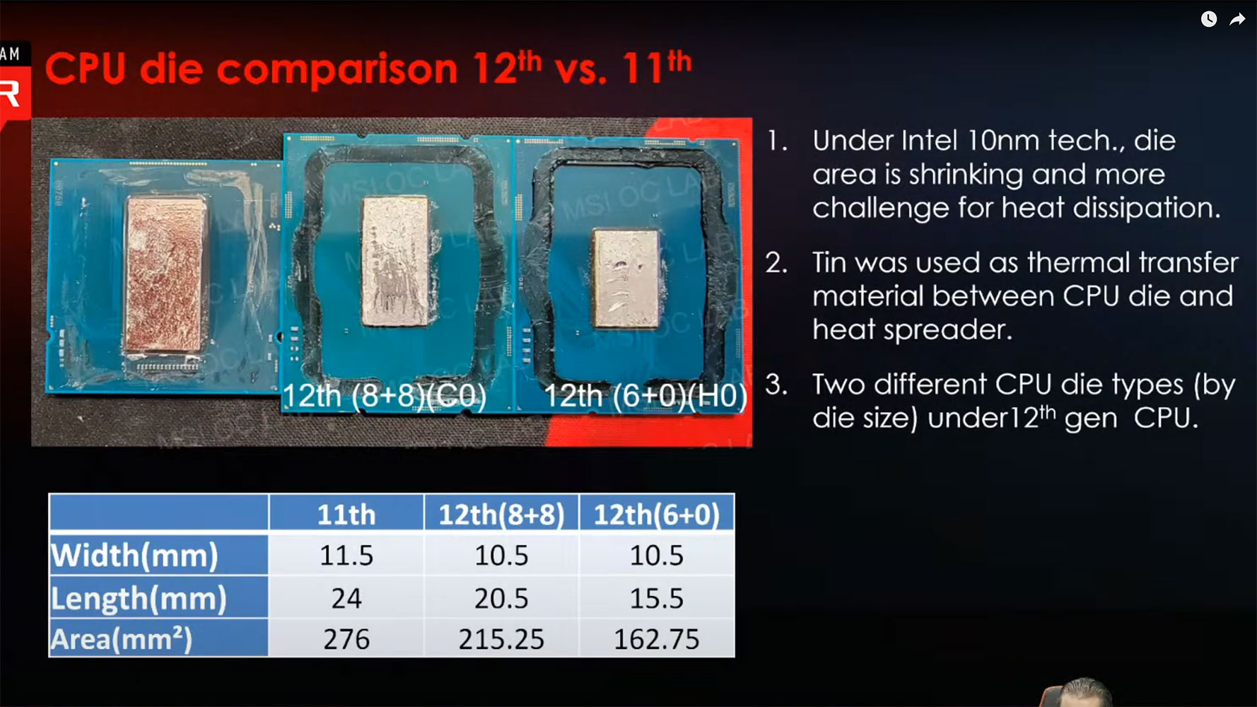
Intel paper-launched the 12th Gen Core processor family on October 27, allowing us to post everything about the processor except performance testing, so we did a more comprehensive Preview Article on the "Alder Lake" microarchitecture. The Core i3-12100F is based on a physically smaller die than the C0 die the i9-12900K is based on, and is codenamed "H0." There are no die-shots from Intel of this die, but MSI OC Lab de-lidded a Core i5 "H0" processor and compared its die-size with that of the larger die. Built on the same Intel 7 node, formerly known as 10 nm Enhanced SuperFin, as the C0 die, the new H0 die is about 24% smaller in area. Considering these are high-volume SKUs, that's a massive savings in wafer consumption at scale.
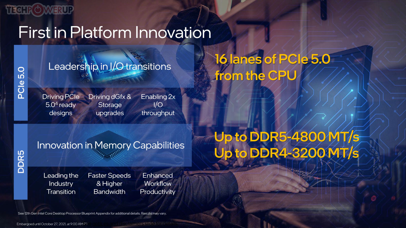
Unlike the C0 die, which physically features 8 "Golden Cove" P-cores and 8 "Gracemont" E-cores, the H0 silicon lacks E-cores and physically only has 6 "Golden Cove" P-cores. With the E-core clusters and a couple of P-cores out of the way, the shared L3 cache size is proportionately reduced to 18 MB. The uncore (integrated northbridge), Xe-LP graphics core, and I/O interfaces are the same as the C0 die. You get 16 lanes of PCI-Express Gen 5 which go toward the PEG slot, 4 lanes of PCI-Express Gen 4 toward a CPU-attached M.2 NVMe slot, and 8 DMI Gen4 lanes toward the chipset bus. The Core i3-12100F features only 4 active P-cores out of the six on the die, and the graphics core is disabled. You'll need a graphics card to go with this processor.

The "Golden Cove" performance core (P-core) features numerical increments to the decode unit, micro-op queue, and micro-op cache. The out-of-order (OoO) engine sees similar increments with 6-wide allocation and 12-wide execution ports, compared to 5-wide allocation and 10-wide execution ports for Cypress Cove. The execution stage sees the addition of a fifth execution port and ALU, FMA with FP16 support, and an updated fast adder (FADD). Similar improvements are made to the cache and memory sub-system. These add toward the 28% IPC uplift for this core.
There are no E-cores physically present on the H0 silicon. With no Hybrid CPU Core architecture present, the Core i5 H0 processor is a traditional multi-core processor that doesn't quite need the Intel Thread Director middleware, although we don't know if Thread Director is absent on these chips or a vestige of it is present.


To eke out the best-possible thermals from the 14 nm node it was stuck with, Intel pulled off some innovative ways to transfer heat between the silicon and cooling solution over the past couple of solutions. These innovations continue with "Alder Lake." The die and STIM are now thinner, and the copper IHS thicker. Among the new overclocking capabilities are the ability to tweak even the E-cores, DDR5 memory, new XMP 3.0 profiles for DDR5 memory, synthetic BCLK that ensures a base-clock overclock doesn't break sensitive clock domains relying on it, and external clock generation, in addition to the processor's internal clock generator. The Core i3-12100F lacks an unlocked multiplier and hence doesn't offer a multiplier value beyond 44x. You could try playing with the 100 MHz base-clock on a Z690 chipset motherboard, as it is de-coupled with other sensitive clock-domains, such as PCIe.
Intel Z690 Chipset

The Z690 chipset is Intel's first client chipset with PCI-Express 4.0 downstream connectivity. It talks to the "Alder Lake-S" processor over the DMI 4.0 x8 chipset bus. Downstream PCIe connectivity includes 12x Gen 4 and 16x Gen 3 PCIe general-purpose lanes. The rest of its chipset-attached connectivity is the same as the Z590, including MIPI SoundWire support, NVMe RAID, 8-port SATA 6 Gbps, and recommended network interfaces that include 2.5 GbE and Wi-Fi 6E.
Intel B660 and H610 Chipsets

As of this writing, VERY few motherboards use the H670 client chipset, making the B660 Intel's mainstream desktop chipset for those with a "locked" 12th Gen Core processor, those who don't need the I/O options of the Z690 and want to save big on the motherboard. The B660 lacks CPU overclocking support, but permits memory overclocking. Motherboard vendors can choose to give it a PCIe Gen 5 PEG slot, as well as DDR5 memory, although you may come across plenty of motherboards with PCIe Gen4 PEG and DDR4 memory. The B660 chipset uses a narrower 4-lane DMI 4.0 chipset bus than what 12th Gen Core processors are capable of (up to 8 DMI 4.0 lanes). This shouldn't be too much of a problem as the chipset only puts out 6 downstream PCIe Gen4 lanes, besides 8 Gen3 lanes. Motherboard designers should use the downstream Gen4 connectivity to wire out another M.2 Gen4 slot. You also get fewer high-bandwidth USB3 port types. The H610 is the bare entry-level chipset. You lose out on memory overclocking, only get Gen3 PCIe connectivity across the board, and no CPU-attached NVMe.
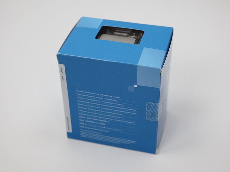
Unboxing and Photography
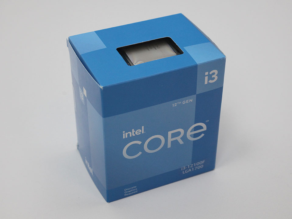
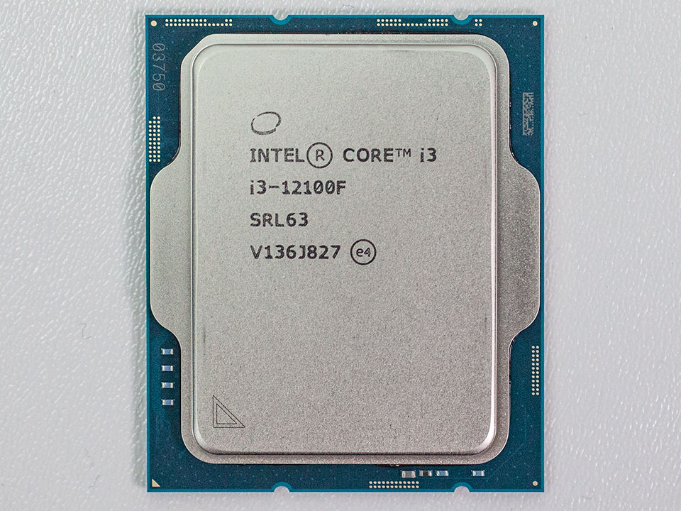
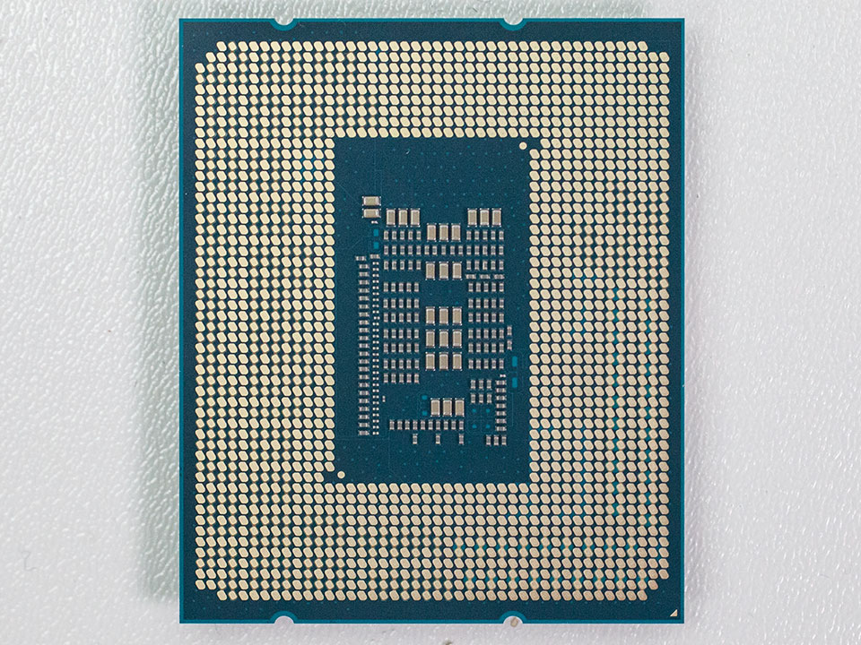
Here it is, the processor itself. It measures 37.5 mm x 45.0 mm and is a more rectangular-looking processor, much like the LGA1366 before it.
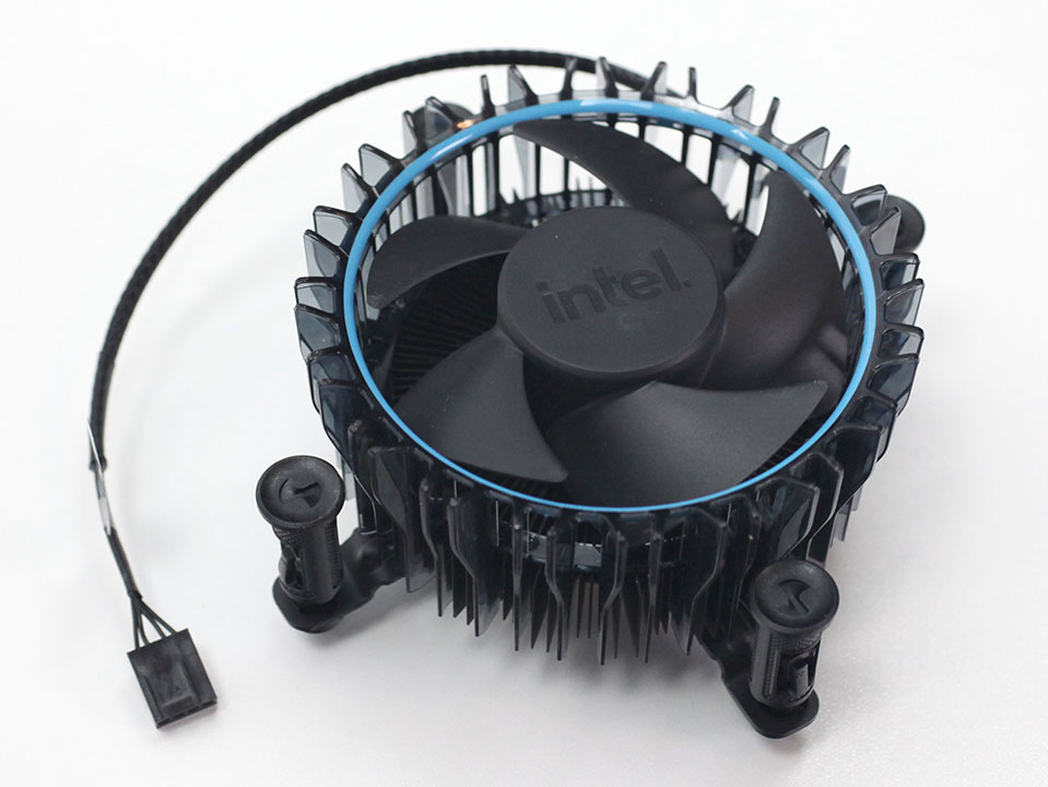
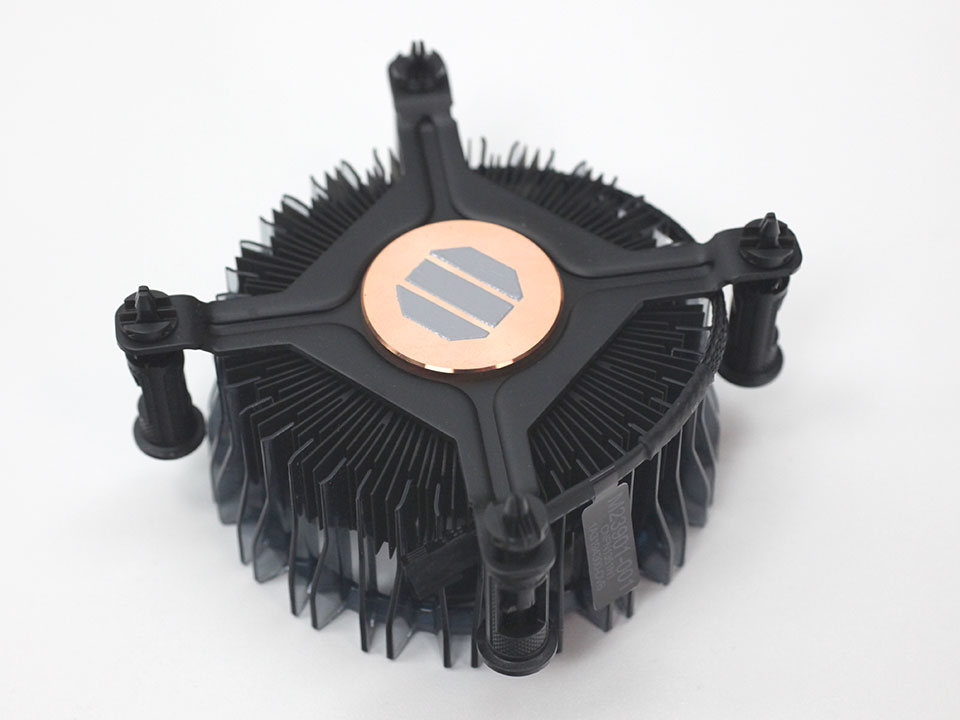

Include in the package is this new Intel stock cooler. It's a relatively simple, compact solution with a copper base.

Intel Socket LGA1700 has an intuitive installation process that should be familiar from many past LGA sockets. Trouble is that it comes with a different cooler mount-hole spacing than LGA1200 and the five different Socket-H series sockets before it, so you'll need to search for a compatible cooler. Most cooler companies are handing out adapters, but these aren't available in all countries.
Test Setup
- All applications, games, and processors are tested with the drivers and hardware listed below—no performance results were recycled between test systems.
- All games and applications are tested using the same version.
- All games are set to their highest quality setting unless indicated otherwise.
| Test System "Alder Lake" | |
|---|---|
| Processor: | All Intel 12th Generation processors |
| Motherboard: | DDR5: ASUS Z690 Maximus Hero / BIOS 0702 DDR4: ASUS Z690 STRIX-A Gaming D4 / BIOS 0705 |
| Memory: | 2x 16 GB G.SKILL Trident Z5 RGB DDR5-6000 36-36-36-76 2T / Gear 2 2x 16 GB G.SKILL Ripjaws V DDR4-3200 16-20-20-34 1T / Gear 1 / DR |
| Graphics: | EVGA GeForce RTX 3080 FTW3 Ultra |
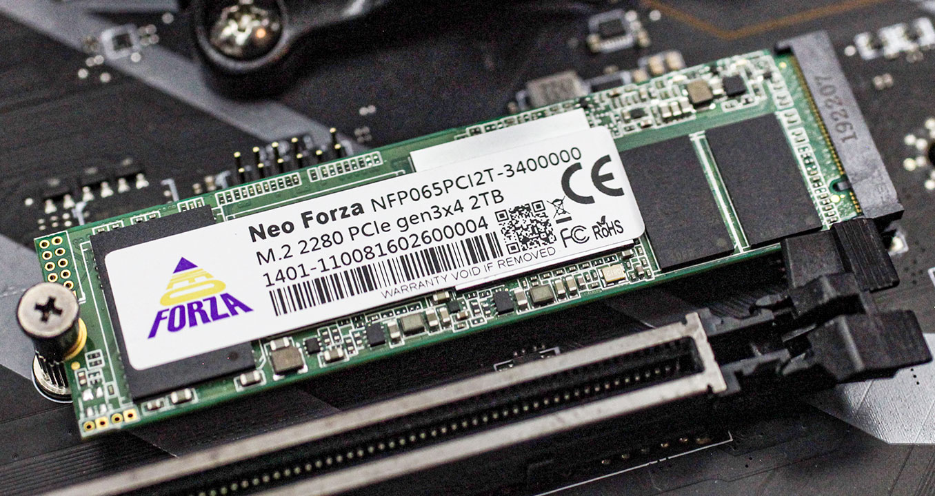
| Storage: | Neo Forza NFP065 1 TB M.2 NVMe SSD |
| Air Cooling: | Noctua NH-U14S |
| Water Cooling: | Arctic Liquid Freezer II 360 mm |
| Thermal Paste: | Arctic MX-5 |
| Power Supply: | Seasonic SS-860XP |
| Software: | Windows 11 Professional 64-bit Build 10.0.22000.282 Includes AMD L3 latency fix |
| Drivers: | NVIDIA GeForce 496.49 WHQL |


| Test System "Zen 3" | |
|---|---|
| Processor: | All AMD Ryzen 5000 |
| Motherboard: | MSI MPG X570 Gaming Plus BIOS 7C37vAF3, AGESA 1.2.0.3c |
| Memory: | 2x 16 GB DDR4-3600 16-20-20-34 1T Infinity Fabric @ 1800 MHz 1:1 |
| All other specifications same as above | |
| Test System "Rocket Lake" | |
|---|---|
| Processor: | All Intel 11th Generation processors |
| Motherboard: | ASUS Z590 Maximus XIII Hero BIOS 1007 |
| Memory: | 2x 16 GB DDR4-3600 16-20-20-34 1T Gear 1 |
| All other specifications same as above | |
| Test System "Comet Lake" | |
|---|---|
| Processor: | All Intel 10th Generation processors |
| Motherboard: | ASUS Z490 Maximus XII Extreme BIOS 2301 |
| Memory: | 2x 16 GB DDR4-3600 16-20-20-34 1T |
| All other specifications same as above | |
Super Pi
SuperPi is one of the most popular benchmarks with overclockers and tweakers. It has been used in world-record competitions since forever. It is a purely single-threaded CPU test that calculates Pi to a large number of digits—32 million for our testing. Released in 1995, it only supports x86 floating-point instructions and thus makes for a good test for single-threaded legacy application performance.
Our Patreon Silver Supporters can read articles in single-page format.
Apr 25th, 2024 01:08 EDT
change timezone
Latest GPU Drivers
New Forum Posts
- Github comments used to push malware via Microsoft repo urls (1)
- What's your latest tech purchase? (20337)
- The Official Linux/Unix Desktop Screenshots Megathread (694)
- XFX RX470 8GB no video and error 43 (27)
- (Anti) SFF fun house (348)
- Cinebench crashed my PC. My Wi-Fi stopped working, and I keep getting a "Please wait" screen when I boot up my PC. (31)
- im new to throttelstop and i think i messed it up by copying others any hints would be very much aprreciated (1)
- Aida64 cache mem OC (7)
- I am getting artifacting when I change Windows security settings. Is my GPU failing, or is this just a Windows issue? (10)
- Is there a technical reason that Windows 11 doesn't have built into it battery charge limitation? (42)
Popular Reviews
- Fractal Design Terra Review
- Thermalright Phantom Spirit 120 EVO Review
- Corsair 2000D Airflow Review
- Minisforum EliteMini UM780 XTX (AMD Ryzen 7 7840HS) Review
- ASUS GeForce RTX 4090 STRIX OC Review
- NVIDIA GeForce RTX 4090 Founders Edition Review - Impressive Performance
- ASUS GeForce RTX 4090 Matrix Platinum Review - The RTX 4090 Ti
- MSI GeForce RTX 4090 Suprim X Review
- MSI GeForce RTX 4090 Gaming X Trio Review
- Gigabyte GeForce RTX 4090 Gaming OC Review
Controversial News Posts
- Sony PlayStation 5 Pro Specifications Confirmed, Console Arrives Before Holidays (116)
- NVIDIA Points Intel Raptor Lake CPU Users to Get Help from Intel Amid System Instability Issues (106)
- AMD "Strix Halo" Zen 5 Mobile Processor Pictured: Chiplet-based, Uses 256-bit LPDDR5X (101)
- US Government Wants Nuclear Plants to Offload AI Data Center Expansion (98)
- Windows 10 Security Updates to Cost $61 After 2025, $427 by 2028 (84)
- Developers of Outpost Infinity Siege Recommend Underclocking i9-13900K and i9-14900K for Stability on Machines with RTX 4090 (84)
- TechPowerUp Hiring: Reviewers Wanted for Motherboards, Laptops, Gaming Handhelds and Prebuilt Desktops (78)
- AMD's RDNA 4 GPUs Could Stick with 18 Gbps GDDR6 Memory (74)