 33
33
Intel Core i7-11700KF Review - Almost as Fast as the 11900K
New OC Features »The Rocket Lake Microarchitecture

The new Rocket Lake microarchitecture forms the bedrock of Intel's 11th Gen Core desktop processor family. The architecture aims to introduce some of Intel's latest CPU and iGPU architectures to the desktop platform. It also brings Deep Learning Boost AI acceleration to this form factor, and AVX-512. With Rocket Lake, Intel aims to introduce their first double-digit, single-threaded CPU performance gains in five years, and a massive iGPU performance gain over the previous generation.

The Rocket Lake-S die is built on what is hopefully the final refinement of Intel's 14 nm silicon fabrication process. Why Intel didn't go with 10 nm SuperFin is anyone's guess. The company still seems to be transitioning between 14 nm and 10 nm-class nodes and is currently prioritizing mobile and enterprise processors with the new node. The price Intel pays for sticking with 14 nm does not just consist of power/thermal costs rivaling 10th Gen Comet Lake. CPU cores are also limited to a maximum of eight since the LGA1200 package has limited fiberglass substrate area.
Rocket Lake combines five key design enhancements over the previous generation. These are the new Cypress Cove CPU core, new Gen12 Xe LP integrated graphics, new Gaussian Network Accelerator (GNA) 2.0—a hardware component that enables the Deep Learning Boost (DLBoost) AI acceleration feature—AVX-512, and, lastly, the updated platform I/O that introduces PCI-Express 4.0, along with a chipset bus with double the width over the previous generation.
Cypress Cove
The new Cypress Cove CPU core is a back-port of the "Sunny Cove" core found in Ice Lake processors, to the 14 nm silicon fabrication node. Sunny Cove was originally designed for Intel's 10 nm node. Intel hasn't released core architecture documentation specific to Cypress Cove, but we can extrapolate from what precious little information Intel put out for Sunny Cove.

A CPU core has essentially three components—the front-end, a part that understands the nature of the work and allocates the right hardware resources to get it done; the Execution stage, where the actual number-crunching happens; and the Load/Store stage, which interfaces this work done/to-be-done with the memory system through the processor's cache hierarchy. Intel appears to have directed its engineering efforts toward improving the Execution and Load/Store stages.
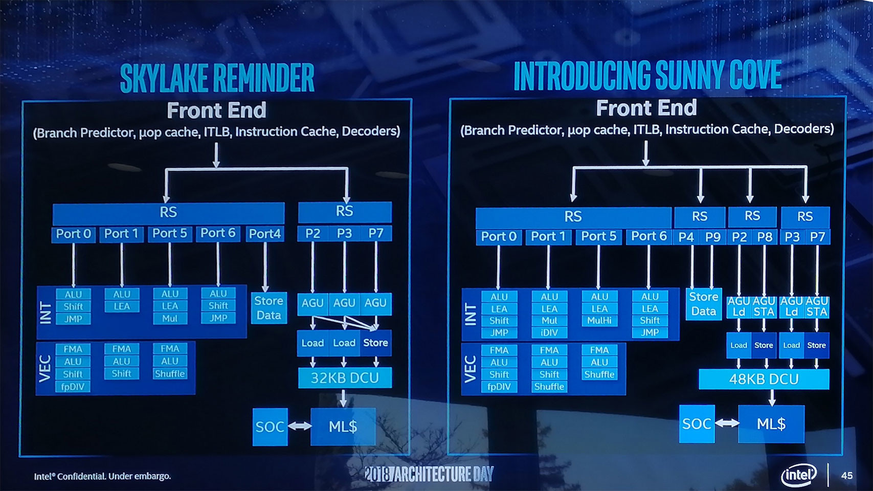

There are numerical increases in key components that make up the Execution stage of the core: 25% more allocation width and execution ports, 33% more AGUs, and an additional Store unit in Load/Store. These changes enable support for newer instruction sets—prominently, 512-bit AVX (or AVX-512). Rocket Lake being a client microarchitecture, receives a truncated version of AVX-512 with only those instructions that are relevant to the client segment. The cache sub-system receives a much needed update with the L1 Data cache being enlarged to 48 KB (from 32 KB on Skylake) and the L2 cache being doubled in size to 512 KB. At 16 MB, the L3 cache size hasn't been changed from the previous-generation 8-core parts.
Intel Xe Graphics

The next major component is the Intel Iris Xe integrated graphics solution based on the latest Gen12 Xe LP graphics architecture. This is the same exact technology as in the Tiger Lake iGPUs, but with a slight difference. While the Tiger Lake iGPU gets 96 execution units as shown in the slide above, the Rocket Lake iGPU only has 48. This was probably done to conserve silicon real-estate on the 14 nm die. Intel attempted to make up for the deficit in EUs compared to Tiger Lake by running the iGPU at higher engine clocks and a more generous power budget than the 15-watt Tiger Lake chips launched so far. In any case, Intel claims that the iGPU on Rocket Lake performs up to 50% faster than the Gen9.5 solution found in Comet Lake. Intel updated the media engine of the iGPU to now offer hardware-acceleration of 10-bit AV1 and 12-bit HEVC video formats.
AVX-512
With this generation, Intel is introducing the new AVX-512 instruction set. This evolution of AVX and AVX2 helps accelerate SIMD workloads—similar operations on a lot of data at the same time. The whole AVX-512 instruction set is a vast set of instructions, not all of which are relevant to the client PC use case. Intel has hence truncated the instruction set, with only certain instructions available to client platforms such as Rocket Lake and Ice Lake, while enterprise/HPC products, such as Xeon Scalar processors and Xeon Phi, have different instructions. Since Cypress Cove is derived from Sunny Cove (and not "Willow Cove"), it features Foundational (F), Conflict-Detect (CD), Vector Propulsion Count (VPOPCNTDQ), Vector Length (VL), BFloat16, Vector-AES, etc., but not the Vector Intersect (VP2INTERSECT) instruction Willow Cove supports.Gaussian Network Accelerator
Next up is GNA 2.0, the hardware component that enables DLBoost, Intel's ambitious new client processor feature that brings AI capabilities to their processor to speed up certain creativity apps that can leverage them. AI-accelerated video and image manipulation has made great strides on smartphones for the past 3+ years, and Intel sees an opportunity for it on the PC, too. DLBoost debuted in 2019 with the 10th Gen Ice Lake mobile processors and is coming to desktop with Rocket Lake. Intel claims that it accelerates deep-learning neural net building/training by up to six times compared to native x86 machine code, which can help offload the CPU cores.PCI-Express 4.0
Lastly, Intel has given the I/O capabilities of Rocket Lake a much-needed upgrade over the previous generation. PCI-Express 4.0 makes its debut. The processor features a 28-lane PCIe root complex. 16 of these go to the PEG port (the main x16 graphics slot), 4 toward an M.2 NVMe Gen 4 slot that's wired directly to the processor (just like on AMD Ryzen platforms), and 8 toward the DMI x8 chipset-bus, which has been doubled in bandwidth compared to the previous generation. These lanes still operate at PCIe Gen 3 bandwidth, as the 500-series PCH doesn't support Gen 4. The memory interface is largely unchanged from Comet Lake. It supports up to 128 GB of dual-channel DDR4 memory and now comes with native support for DDR4-3200. The integrated memory controller behind the interface, though, is significantly improved, as we'll detail on the next page.Intel Z590 Chipset
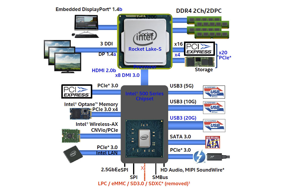
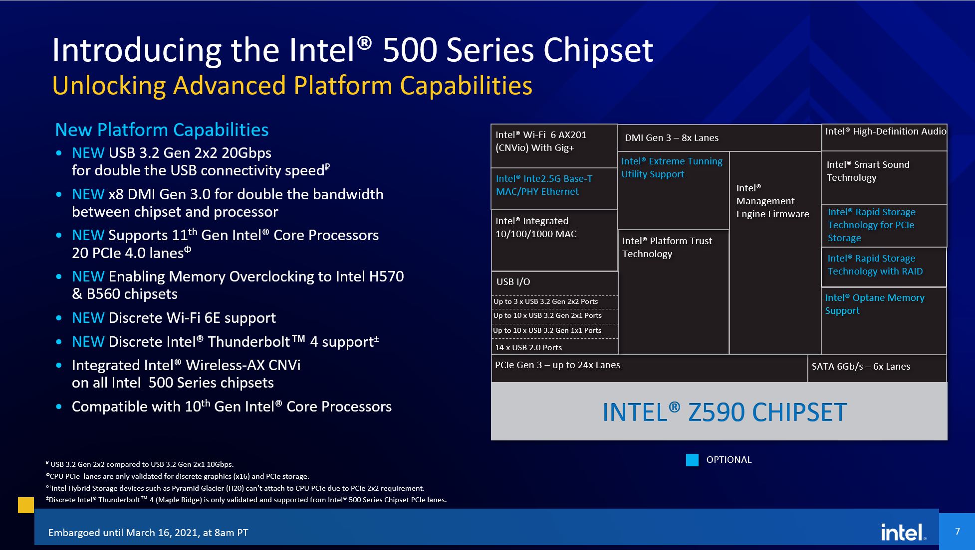
The Z590 chipset is based on a new silicon, and isn't just a refresh of the Z490. Built on the 14 nm silicon fabrication node, it now supports the DMI 3.0 x8 chipset bus, which offers 128 Gbps of bi-directional bandwidth, double that of the previous generation, when paired with a 11th Gen Rocket Lake processor. The chipset also supports the older 10th Gen Comet Lake processor, but the DMI will run at a width of four lanes. Downstream PCIe I/O is the same as with the Z490, with 28 PCI-Express 3.0 lanes.
What has changed is native USB 3.2x2 (20 Gbps), USB audio offload with the HSP of compatible USB DACs being performed on the chipset and not the CPU, and the all-new Intel MIPI SoundWire audio interface. An evolution of the now 18-year-old HD Audio bus, SoundWire enables low-power audio capabilities when the PC is standing by—for such use cases as voice assistants. While not strictly a function of the chipset, the recommendation for 500-series chipsets is to pair them with Intel's latest Wi-Fi 6E WLAN controllers, discrete Thunderbolt 4 controllers, and the latest stepping of its 2.5 GbE chips.
Apr 19th, 2024 20:46 EDT
change timezone
Latest GPU Drivers
New Forum Posts
- USB C to USB A hub (42)
- The Official Linux/Unix Desktop Screenshots Megathread (688)
- GTX 1060 6GB ASUS GPU Shuts Down after 5min of Gaming (3)
- Official Board Game Discussion (0)
- AMD RX 7000 series GPU Owners' Club (1068)
- I just succesfully baked DDR4 (69)
- I9 13890HX undervolting Suggestions (4)
- Undervolting Dell XPS 14 9440 is it possible? (7)
- Share your AIDA 64 cache and memory benchmark here (2884)
- Roccat Kone AIMO has developed a double left click, when I click it once. Any fix out there? (34)
Popular Reviews
- Horizon Forbidden West Performance Benchmark Review - 30 GPUs Tested
- Fractal Design Terra Review
- Corsair 2000D Airflow Review
- Thermalright Phantom Spirit 120 EVO Review
- Minisforum EliteMini UM780 XTX (AMD Ryzen 7 7840HS) Review
- Creative Pebble X Plus Review
- FiiO KB3 HiFi Mechanical Keyboard Review - Integrated DAC/Amp!
- ASUS GeForce RTX 4090 STRIX OC Review
- NVIDIA GeForce RTX 4090 Founders Edition Review - Impressive Performance
- ASUS GeForce RTX 4090 Matrix Platinum Review - The RTX 4090 Ti
Controversial News Posts
- Sony PlayStation 5 Pro Specifications Confirmed, Console Arrives Before Holidays (111)
- NVIDIA Points Intel Raptor Lake CPU Users to Get Help from Intel Amid System Instability Issues (102)
- US Government Wants Nuclear Plants to Offload AI Data Center Expansion (98)
- AMD "Strix Halo" Zen 5 Mobile Processor Pictured: Chiplet-based, Uses 256-bit LPDDR5X (84)
- Windows 10 Security Updates to Cost $61 After 2025, $427 by 2028 (82)
- Developers of Outpost Infinity Siege Recommend Underclocking i9-13900K and i9-14900K for Stability on Machines with RTX 4090 (82)
- TechPowerUp Hiring: Reviewers Wanted for Motherboards, Laptops, Gaming Handhelds and Prebuilt Desktops (72)
- Intel Realizes the Only Way to Save x86 is to Democratize it, Reopens x86 IP Licensing (70)