 59
59
Intel Core i7-12700K Review - Almost as Fast as the i9-12900K
(59 Comments) »Introduction
The Core i7-12700K "Alder Lake" is a performance desktop processor Intel priced around the $400-mark. It succeeds a long line of top mainstream desktop processors by the company that dominated the segment for over a decade. It's only with the past three generations that Intel introduced the Core i9 extension to the desktop segment to sell top-tier processors around the $500-mark. The i7-12700K is technically a 12-core/20-thread processor, but there's a lot more to that core count. "Alder Lake" debuts the hybrid core topology to the desktop segment, combining a number of bigger "performance" cores, or P-cores, with smaller "efficiency" cores, or E-cores.

The Core i7-12700K features eight P-cores and four E-cores. HyperThreading is enabled on the P-cores, which works out to the 12-core/20-thread count. Built on the Intel 7 (10 nm Enhanced SuperFin) silicon fabrication node, which offers comparable transistor-density and power characteristics to 7 nm-class nodes by TSMC, the "Alder Lake-S" silicon features up to 8 "Golden Cove" P-cores and up to 8 "Gracemont" E-cores, of which all 8 P-cores and 4 out of 8 E-cores are enabled on the i7-12700K.
Intel claims the "Golden Cove" performance cores offer a massive 28% IPC gain over the "Skylake" cores powering Intel processors for a bulk of the last decade, and 19% over the "Cypress Cove" cores powering the 11th Gen "Rocket Lake" processors. The "Gracemont" efficiency cores take up a quarter of the die area and a fraction of the power of the P-cores, but at the right clock speed are able to match the "Skylake" core in IPC. Intel has also adjusted the instruction sets available to the two core types for a high degree of ISA coherency between the two core types. The Intel Thread Director technology is a hardware middleware that interfaces with the operating system at a very low level and ensures the right workload distribution to the two core types.
The Core i7-12700K is clocked at 3.60 GHz base and 5.00 GHz max boost for the P-cores, and 2.70 GHz base with 3.80 GHz boost for the E-cores. The processor features a total of 14 MB of L2 cache. That's 1.25 MB per P-core, and 2 MB for the E-core cluster. 25 MB of L3 cache is shared between both the core types. As an unlocked K-SKU, you get the ability to easily overclock both core types, as well as the integrated graphics. The Intel UHD 770 iGPU is based on the same Xe LP graphics architecture as the UHD 750 found in 11th Gen "Rocket Lake" processors, down to the same execution unit count of 32. All that has chanced is an increase in the iGPU frequency to 1.55 GHz from 1.30 GHz.
With "Alder Lake," Intel is dispensing with TDP as a measure of power or thermals. The processor now comes with two monikers you should be aware of, the Processor Base Power value, which is set at 125 W, and Maximum Turbo Power value, which is 190 W for the i7-12700K. Several power levels span the two, but what's relevant is that you can get the processor to run at its maximum turbo power value indefinitely.
The Core i7-12700K has its sights set on the likes of the AMD Ryzen 9 5900X and Ryzen 7 5800X and priced competitively to the two. The processor supports both the newer DDR5 memory and current DDR4 memory, and Intel ensured its motherboard partners launch plenty of options for those wanting to keep their older memory sticks. The processor also features new cutting-edge PCI-Express Gen 5, though only for the main x16 graphics slot. The processor-attached M.2 NVMe slot is still Gen 4. We find out whether Intel has managed to score a win around the $400-mark, which would spell trouble for one of AMD's best-selling segments among enthusiasts.
| Price | Cores / Threads | Base Clock | Max. Boost | L3 Cache | TDP | Architecture | Process | Socket | |
|---|---|---|---|---|---|---|---|---|---|
| Core i5-9400F | $170 | 6 / 6 | 2.9 GHz | 4.1 GHz | 9 MB | 65 W | Coffee Lake | 14 nm | LGA 1151 |
| Core i5-10400F | $180 | 6 / 12 | 2.9 GHz | 4.3 GHz | 12 MB | 65 W | Comet Lake | 14 nm | LGA 1200 |
| Core i5-11400F | $215 | 6 / 12 | 2.6 GHz | 4.4 GHz | 12 MB | 65 W | Rocket Lake | 14 nm | LGA 1200 |
| Core i5-10500 | $225 | 6 / 12 | 3.1 GHz | 4.5 GHz | 12 MB | 65 W | Comet Lake | 14 nm | LGA 1200 |
| Ryzen 5 3600 | $230 | 6 / 12 | 3.6 GHz | 4.2 GHz | 32 MB | 65 W | Zen 2 | 7 nm | AM4 |
| Core i5-9600K | $210 | 6 / 6 | 3.7 GHz | 4.6 GHz | 9 MB | 95 W | Coffee Lake | 14 nm | LGA 1151 |
| Core i5-10600K | $260 | 6 / 12 | 4.1 GHz | 4.8 GHz | 12 MB | 125 W | Comet Lake | 14 nm | LGA 1200 |
| Core i5-11600K | $260 | 6 / 12 | 3.9 GHz | 4.9 GHz | 12 MB | 125 W | Rocket Lake | 14 nm | LGA 1200 |
| Ryzen 5 3600X | $290 | 6 / 12 | 3.8 GHz | 4.4 GHz | 32 MB | 95 W | Zen 2 | 7 nm | AM4 |
| Ryzen 5 5600G | $250 | 6 / 12 | 3.9 GHz | 4.4 GHz | 16 MB | 65 W | Zen 3 + Vega | 7 nm | AM4 |
| Ryzen 5 5600X | $310 | 6 / 12 | 3.7 GHz | 4.6 GHz | 32 MB | 65 W | Zen 3 | 7 nm | AM4 |
| Core i5-12600K | $300 | 6+4 / 16 | 3.7 / 2.8 GHz | 4.9 / 3.6 GHz | 20 MB | 125 W | Alder Lake | 10 nm | LGA 1700 |
| Core i7-9700K | $310 | 8 / 8 | 3.6 GHz | 4.9 GHz | 12 MB | 95 W | Coffee Lake | 14 nm | LGA 1151 |
| Core i7-10700K | $330 | 8 / 16 | 3.8 GHz | 5.1 GHz | 16 MB | 125 W | Comet Lake | 14 nm | LGA 1200 |
| Core i7-11700K | $350 | 8 / 16 | 3.6 GHz | 5.0 GHz | 16 MB | 125 W | Rocket Lake | 14 nm | LGA 1200 |
| Ryzen 7 3700X | $320 | 8 / 16 | 3.6 GHz | 4.4 GHz | 32 MB | 65 W | Zen 2 | 7 nm | AM4 |
| Ryzen 7 5700G | $350 | 8 / 16 | 3.8 GHz | 4.6 GHz | 16 MB | 65 W | Zen 3 + Vega | 7 nm | AM4 |
| Ryzen 7 3800XT | $400 | 8 / 16 | 3.9 GHz | 4.7 GHz | 32 MB | 105 W | Zen 2 | 7 nm | AM4 |
| Core i7-12700K | $420 | 8+4 / 20 | 3.6 / 2.7 GHz | 5.0 / 3.8 GHz | 25 MB | 125 W | Alder Lake | 10 nm | LGA 1700 |
| Ryzen 7 5800X | $400 | 8 / 16 | 3.8 GHz | 4.7 GHz | 32 MB | 105 W | Zen 3 | 7 nm | AM4 |
| Core i9-10900 | $440 | 10 / 20 | 2.8 GHz | 5.2 GHz | 20 MB | 65 W | Comet Lake | 14 nm | LGA 1200 |
| Ryzen 9 3900X | $430 | 12 / 24 | 3.8 GHz | 4.6 GHz | 64 MB | 105 W | Zen 2 | 7 nm | AM4 |
| Ryzen 9 5900X | $525 | 12 / 24 | 3.7 GHz | 4.8 GHz | 64 MB | 105 W | Zen 3 | 7 nm | AM4 |
| Core i9-9900K | $470 | 8 / 16 | 3.6 GHz | 5.0 GHz | 16 MB | 95 W | Coffee Lake | 14 nm | LGA 1151 |
| Core i9-10900K | $470 | 10 / 20 | 3.7 GHz | 5.3 GHz | 20 MB | 125 W | Comet Lake | 14 nm | LGA 1200 |
| Core i9-11900K | $550 | 8 / 16 | 3.5 GHz | 5.3 GHz | 16 MB | 125 W | Rocket Lake | 14 nm | LGA 1200 |
| Ryzen 9 3950X | $765 | 16 / 32 | 3.5 GHz | 4.7 GHz | 64 MB | 105 W | Zen 2 | 7 nm | AM4 |
| Ryzen 9 5950X | $750 | 16 / 32 | 3.4 GHz | 4.9 GHz | 64 MB | 105 W | Zen 3 | 7 nm | AM4 |
| Core i9-12900K | $600 | 8+8 / 24 | 3.2 / 2.4 GHz | 5.2 / 3.9 GHz | 30 MB | 125 W | Alder Lake | 10 nm | LGA 1700 |
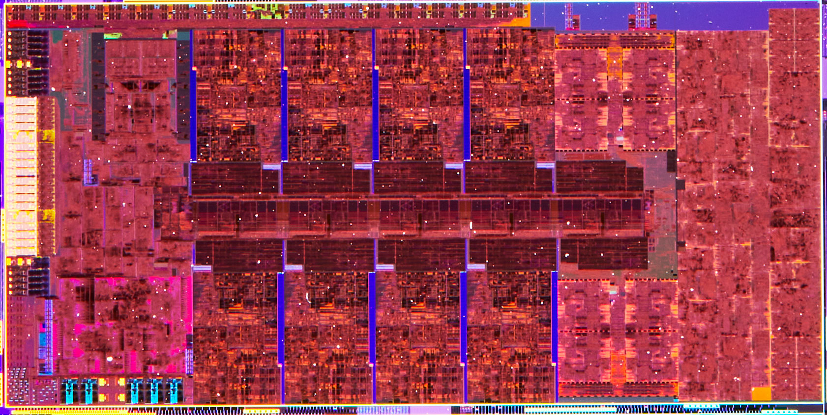
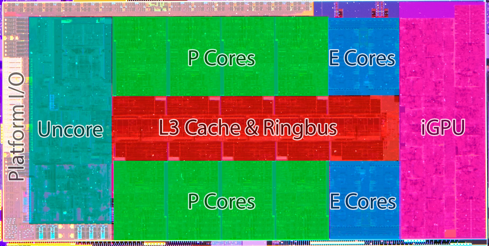
Intel paper-launched the 12th Gen Core processor family on October 27, allowing us to post everything about the processor except performance testing, so we did a more comprehensive Preview Article on the "Alder Lake" microarchitecture. "Alder Lake-S" is the first desktop processor silicon built by Intel on its Intel 7 silicon fabrication node, formerly known as 10 nm Enhanced SuperFin. This node offers transistor-density and power characteristics comparable to 7 nm-class nodes by TSMC. The die measures approximately 200 mm², although it is noticeably smaller than the 14 nm "Rocket Lake-S" die.
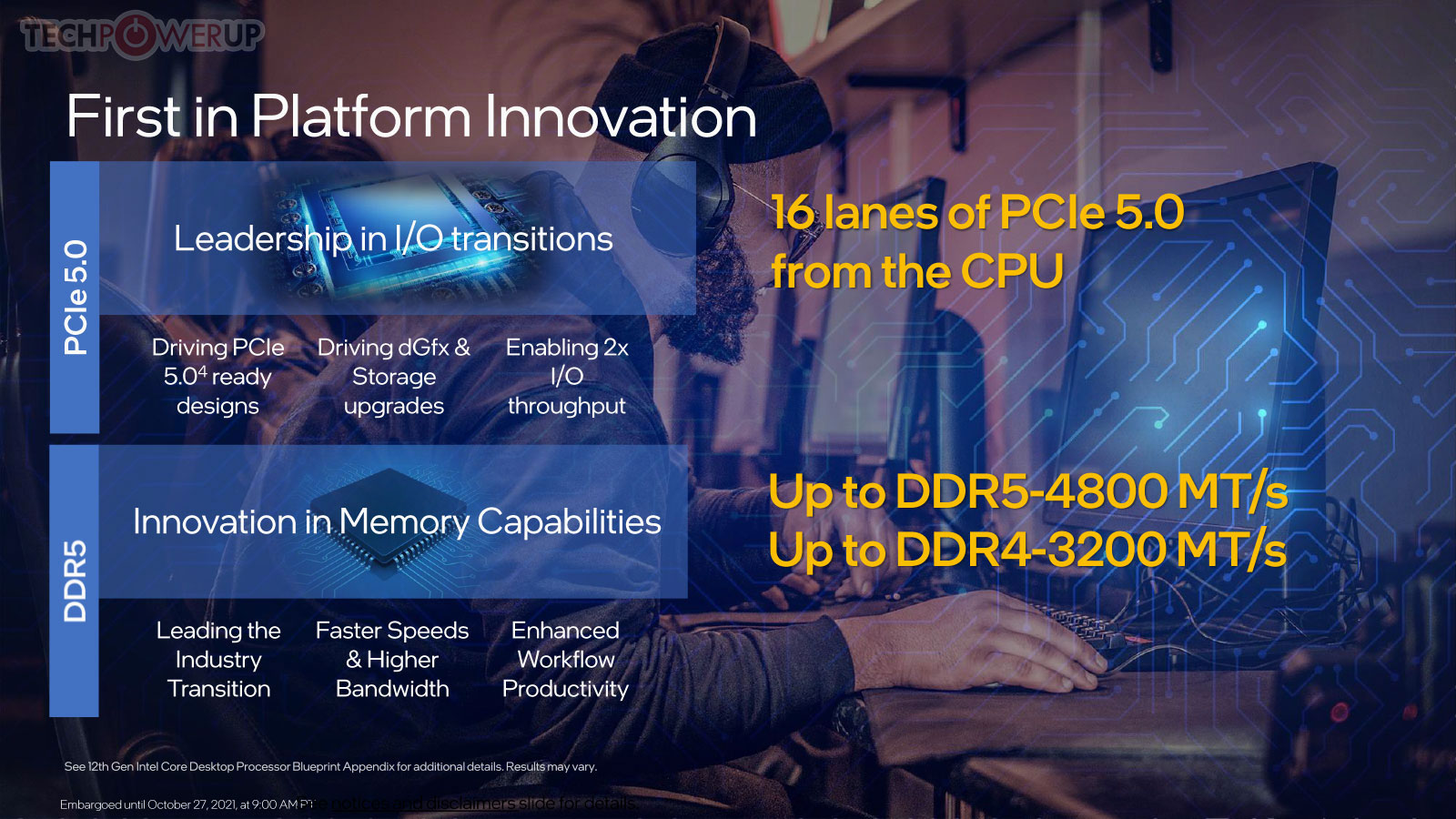
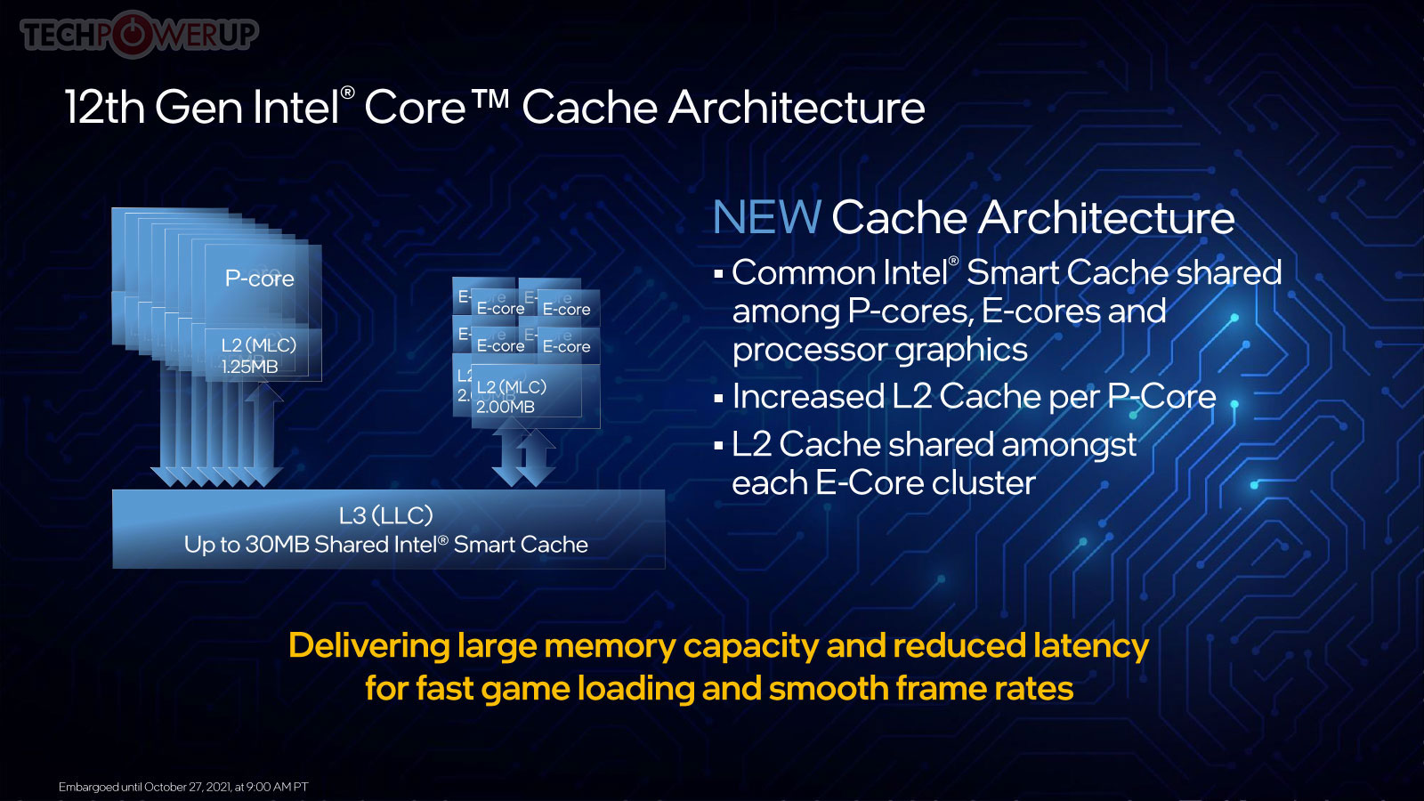
The monolithic silicon features 8 "Golden Cove" P and 8 "Gracemont" E-cores. The E-cores are spread across two 4-core "E-core Clusters." A bi-directional Ringbus and 30 MB of L3 cache connect the P-cores, and E-core clusters, with the Uncore (integrated northbridge) and iGPU. The chip features a dual-mode memory controller that supports 160-bit wide DDR5 (native support for DDR5-4800),or 128-bit wide DDR4 (native support for DDR4-3200). The Gen12 Xe LP iGPU is carried over almost unchanged from the "Rocket Lake-S" silicon, with a minor speed-bump. The PCI-Express root complex is fascinating. The silicon puts out 16 Gen 5 lanes (32 Gbps per lane), which are allocated to the PEG slot on the motherboard; and 12 Gen 4 lanes (16 Gbps per lane) from which four drive a CPU-attached M.2 NVMe slot and eight serve as physical layer of the DMI 4.0 x8 chipset bus (128 Gbps per direction bandwidth).
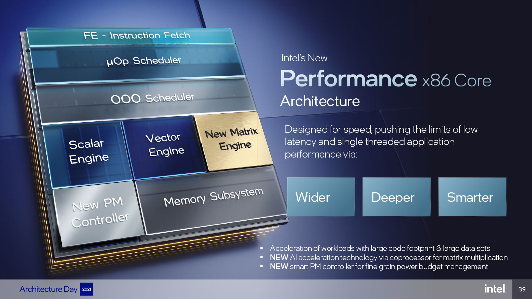

The "Golden Cove" performance core (P-core) features numerical increments to the decode unit, micro-op queue, and micro-op cache. The out-of-order (OoO) engine sees similar increments with 6-wide allocation and 12-wide execution ports, compared to 5-wide allocation and 10-wide execution ports for Cypress Cove. The execution stage sees the addition of a fifth execution port and ALU, FMA with FP16 support, and an updated fast adder (FADD). Similar improvements are made to the cache and memory sub-system. These add toward the 28% IPC uplift for this core. The E-core, on the other hand, is designed to provide a massive performance uplift from the previous-generation "Tremont" low-power microarchitecture, mainly to give it certain ISA capabilities found in larger cores, such as AVX2. The front-end is upgraded by a double-size 64 KB L1 instruction cache, more powerful branch-prediction unit, and two sets of triple out-of-order decoders. The out-of-order engine features a wide 256-entry OoO window and 17 execution ports for more parallelism. The execution stage sees a near 33% increase in both scalar and vector execution stages, as well as double the load store.
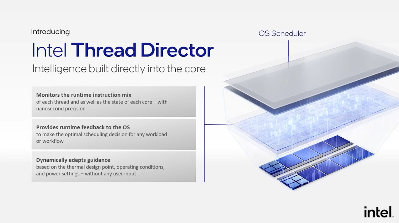
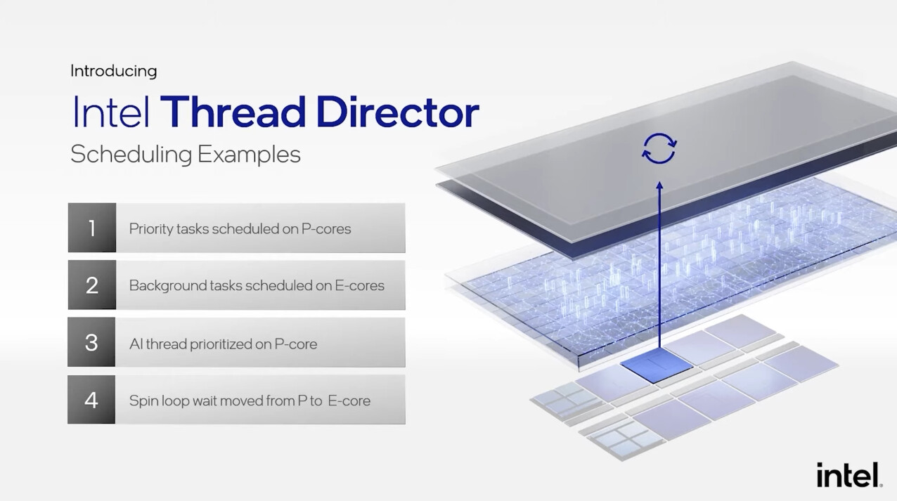
Intel Thread Director is a vital component that ensures the operating system doesn't see Alder Lake as having the same kind of CPU cores, sending processing traffic uniformly to all cores. Instead, it gives the OS a degree of awareness of the Hybrid architecture and ensures certain kinds of tasks are allocated exclusively on P-cores, and others on E-cores. It also senses the nature of the processing workload (whether it's running in the foreground or background), and decides which kind of cores to tie it to. The OS scheduler by itself moves traffic between cores to meet certain power/thermal objectives, but Thread Director ensures this movement doesn't break the core-type hierarchy. Windows 11 is the recommended version of Windows for Alder Lake, as it introduces the ability for software to inform the processor of the nature of its work, and the kind of cores it's comfortable getting processed by.

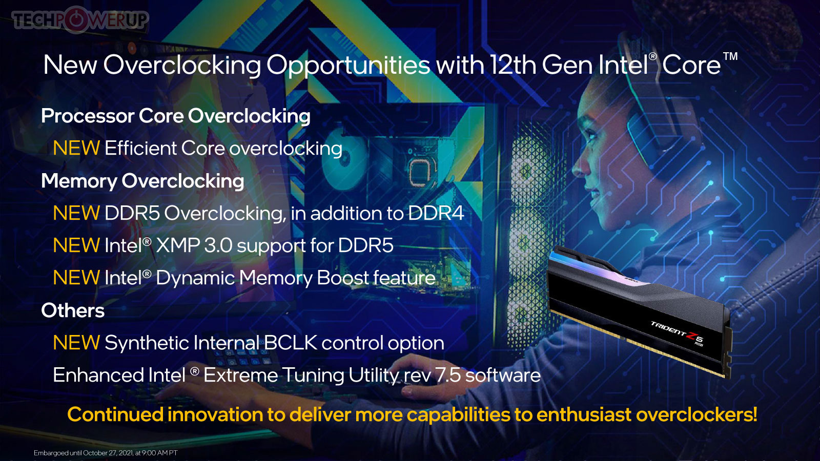
Over the past couple of solutions, Intel pulled off some innovative ways to transfer heat between the silicon and cooling solution to eke out the best possible thermals from the 14 nm node it was stuck with. These innovations continue with Alder Lake. The die and STIM are now thinner, and the copper IHS thicker. Among the new overclocking capabilities are the ability to tweak even the E-cores, DDR5 memory, new XMP 3.0 profiles for DDR5 memory, synthetic BCLK that ensures a base-clock overclock doesn't break sensitive clock domains that rely on it, and external clock generation, in addition to the processor's internal clock generator.


With the monolithic silicon gaining complexity, there are several new overclocking knobs and clock domains to maximize your overclock. The introduction of the E-core adds its own base-clock multiplier, called xE, which works separately from the core ratio of the P-cores, dubbed xP. The xG multiplier dictates iGPU frequency. xR dictates the frequency at which the Ringbus interconnect and L3 cache operate.
Intel Z690 Chipset

Intel is debuting its 12th Gen Core desktop processors in 2021 exclusively with only the unlocked "K" and "KF" variants, so it's only launching the companion Z690 chipset. The "locked" processor SKUs and value-ended chipsets are expected to join the product stack in 2022. The Z690 chipset is Intel's first client chipset with PCI-Express 4.0 downstream connectivity. It talks to the "Alder Lake-S" processor over the DMI 4.0 x8 chipset bus. Downstream PCIe connectivity includes 12x Gen 4 and 16x Gen 3 PCIe general-purpose lanes. The rest of its chipset-attached connectivity is the same as on Z590, including MIPI SoundWire support, NVMe RAID, 8-port SATA 6 Gbps, and the recommended network interfaces that include 2.5 GbE and Wi-Fi 6E.
Unboxing and Photography
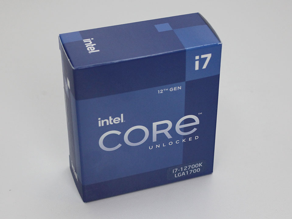
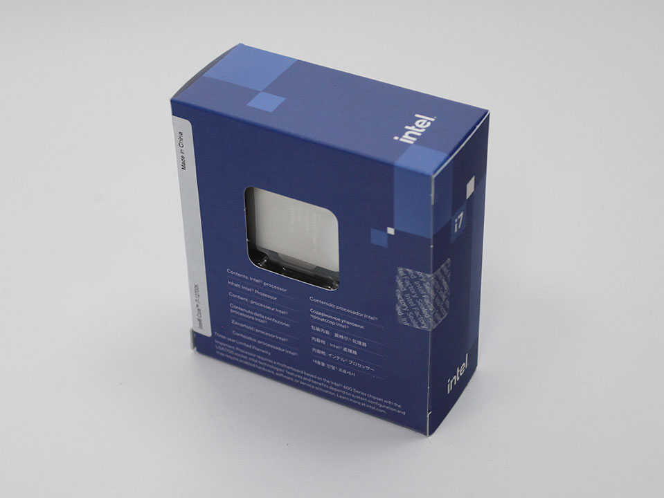
The Core i7-12700K retail box is extremely spartan and probably doesn't even cost a dollar to make. It's a simple paperboard box with a plastic blister inside that holds the processor, some papers, and the case badge.
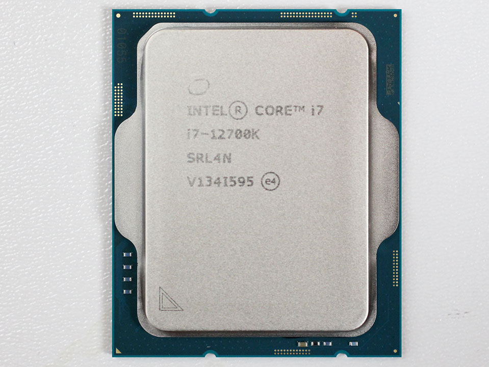

Here it is, the processor itself. It measures 37.5 mm x 45.0 mm and is a more rectangular-looking processor, much like the LGA1366 before it.

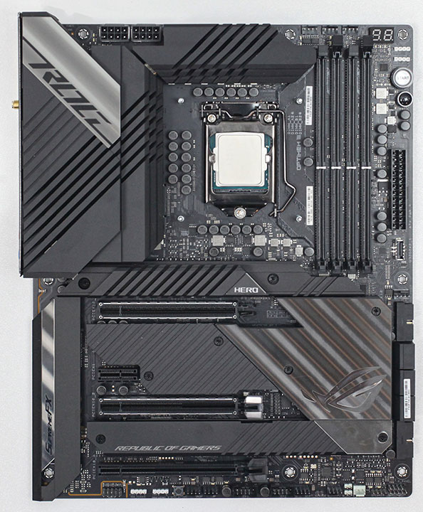
Intel Socket LGA1700 has an intuitive installation process that should be familiar from many past LGA sockets. Trouble is that it comes with a different cooler mount-hole spacing than LGA1200 and five different Socket-H series sockets before it, so you'll need to search for a compatible cooler. Most cooler companies are handing out adapters, but these aren't available in all countries.
Test Setup
- All applications, games, and processors are tested with the drivers and hardware listed below—no performance results were recycled between test systems.
- All games and applications are tested using the same version.
- All games are set to their highest quality setting unless indicated otherwise.
| Test System "Alder Lake" | |
|---|---|
| Processor: | All Intel 12th Generation processors |
| Motherboard: | ASUS Z690 Maximus Hero BIOS 0702 |
| Memory: | 2x 16 GB G.SKILL Trident Z5 RGB DDR5-6000 36-36-36-76 2T Gear 2 |
| Graphics: | EVGA GeForce RTX 3080 FTW3 Ultra |
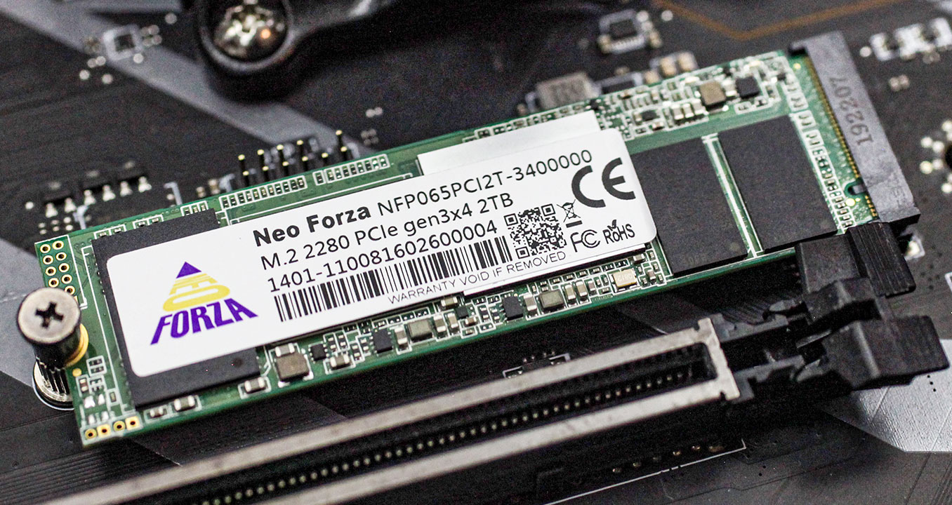
| Storage: | Neo Forza NFP065 1 TB M.2 NVMe SSD |
| Air Cooling: | Noctua NH-U14S |
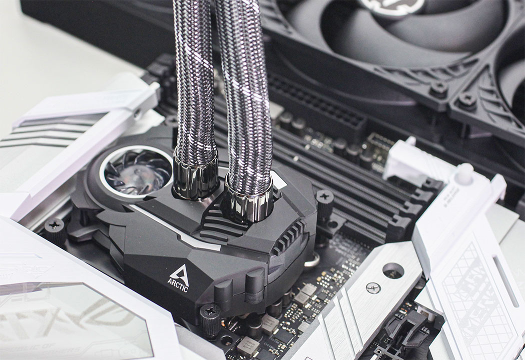
| Water Cooling: | Arctic Liquid Freezer II 360 mm |
| Thermal Paste: | Arctic MX-5 |
| Power Supply: | Seasonic SS-860XP |
| Software: | Windows 11 Professional 64-bit Build 10.0.22000.282 Includes AMD L3 latency fix |
| Drivers: | NVIDIA GeForce 496.49 WHQL |


| Test System "Zen 3" | |
|---|---|
| Processor: | All AMD Ryzen 5000 |
| Motherboard: | MSI MPG X570 Gaming Plus BIOS 7C37vAF3, AGESA 1.2.0.3c |
| Memory: | 2x 16 GB DDR4-3600 16-20-20-34 1T Infinity Fabric @ 1800 MHz 1:1 |
| All other specifications same as above | |
| Test System "Rocket Lake" | |
|---|---|
| Processor: | All Intel 11th Generation processors |
| Motherboard: | ASUS Z590 Maximus XIII Hero BIOS 1007 |
| Memory: | 2x 16 GB DDR4-3600 16-20-20-34 1T Gear 1 |
| All other specifications same as above | |
| Test System "Comet Lake" | |
|---|---|
| Processor: | All Intel 10th Generation processors |
| Motherboard: | ASUS Z490 Maximus XII Extreme BIOS 2301 |
| Memory: | 2x 16 GB DDR4-3600 16-20-20-34 1T |
| All other specifications same as above | |
Super Pi
SuperPi is one of the most popular benchmarks with overclockers and tweakers. It has been used in world-record competitions since forever. It is a purely single-threaded CPU test that calculates Pi to a large number of digits—32 million for our testing. Released in 1995, it only supports x86 floating-point instructions and thus makes for a good test for single-threaded legacy application performance.
wPrime
While SuperPi focuses on calculating Pi, wPrime tackles another mathematical problem: finding prime numbers. It uses Newton's Method for that. One of the design goals for wPrime was to engineer it so that it can make the best use of all cores and threads available on a processor.
Our Patreon Silver Supporters can read articles in single-page format.
Apr 26th, 2024 07:19 EDT
change timezone
Latest GPU Drivers
New Forum Posts
- Best SSD for system drive (85)
- The Official Linux/Unix Desktop Screenshots Megathread (695)
- Horizontal black lines popping up on my screen? (9)
- What's your latest tech purchase? (20347)
- Share your AIDA 64 cache and memory benchmark here (2918)
- Secure boot already open help (1)
- What are you playing? (20535)
- TPU's Nostalgic Hardware Club (18472)
- Last game you purchased? (258)
- Alphacool CORE 1 CPU block - bulging with danger of splitting? (22)
Popular Reviews
- HYTE THICC Q60 240 mm AIO Review
- MOONDROP x Crinacle DUSK In-Ear Monitors Review - The Last 5%
- Alienware Pro Wireless Gaming Keyboard Review
- Upcoming Hardware Launches 2023 (Updated Feb 2024)
- Thermalright Phantom Spirit 120 EVO Review
- ASUS Radeon RX 7900 GRE TUF OC Review
- RTX 4090 & 53 Games: Ryzen 7 5800X vs Ryzen 7 5800X3D Review
- FiiO K19 Desktop DAC/Headphone Amplifier Review
- NVIDIA RTX 4090: 450 W vs 600 W 12VHPWR - Is there any notable performance difference?
- RTX 4090 & 53 Games: Core i9-13900K vs Ryzen 7 5800X3D Review
Controversial News Posts
- Windows 11 Now Officially Adware as Microsoft Embeds Ads in the Start Menu (123)
- Sony PlayStation 5 Pro Specifications Confirmed, Console Arrives Before Holidays (117)
- NVIDIA Points Intel Raptor Lake CPU Users to Get Help from Intel Amid System Instability Issues (106)
- AMD "Strix Halo" Zen 5 Mobile Processor Pictured: Chiplet-based, Uses 256-bit LPDDR5X (101)
- US Government Wants Nuclear Plants to Offload AI Data Center Expansion (98)
- AMD's RDNA 4 GPUs Could Stick with 18 Gbps GDDR6 Memory (89)
- Developers of Outpost Infinity Siege Recommend Underclocking i9-13900K and i9-14900K for Stability on Machines with RTX 4090 (85)
- Windows 10 Security Updates to Cost $61 After 2025, $427 by 2028 (84)