 209
209
Intel Core i9-10900K Review - World's Fastest Gaming Processor
Test Setup »Architecture
Under the hood of the Core i9-10900K is the 10-core "Comet Lake-S" silicon, built on the same 14 nm++ process as the previous two generations, but with one key difference.
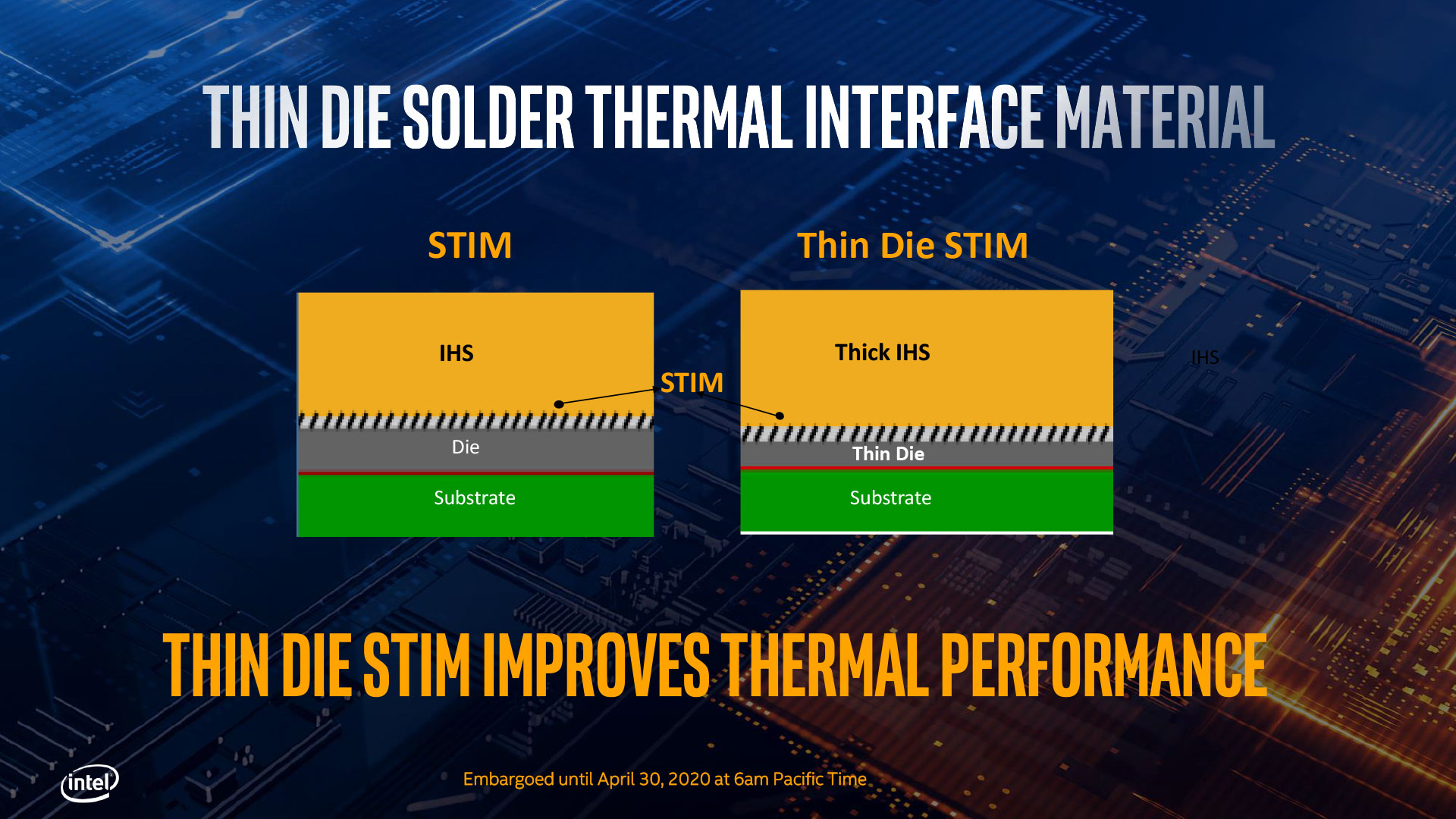
Intel physically thinned the die along the Z-axis by removing as much of the silicon bulk as possible, the idea being that heat generated by the die travels through less silicon. The more conductive copper integrated heatspreader has been made thicker, and a solder thermal interface material (STIM) is used between the two. The die area is estimated by AnandTech to be around 198.4 mm², and from the looks of it, Intel can't add any more cores on this package by stretching the die without chopping off the iGPU.
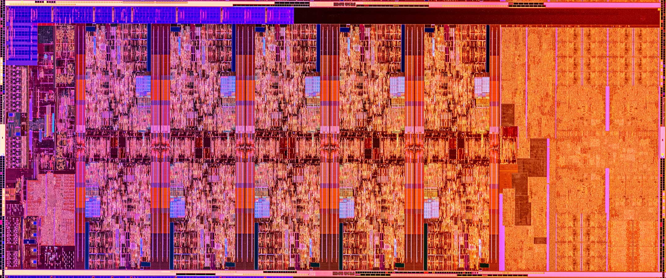
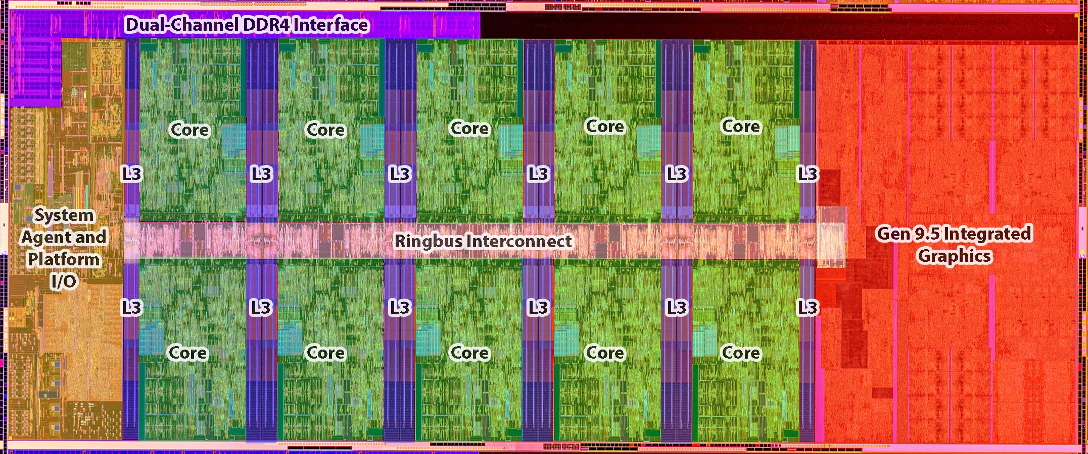
The "Comet Lake-S" silicon is laid out similar to the past four generations of Intel mainstream processors, with two rows of CPU cores flanked by the iGPU on one side and the system agent (integrated northbridge) on the other, and a Ringbus Interconnect serving as the town square between the various components. The last-level cache is scattered across as slices of 1 MB or 2 MB, adding up to 20 MB of unified L3 cache that's equally accessible to all cores. It's fascinating to see how Intel retained its Ringbus-based multi-core design for this generation instead of designing something with its new Mesh interconnect. Intel still hasn't reached the core-count barrier beyond which the Ringbus has to be junked in favor of Mesh Interconnect tiles, lest it suffer the detrimental effects of ringbus latencies.
Much of the processor's uncore components are clumped into the System Agent, which contains the memory controller, PCI-Express gen 3.0 root-complex, DMI interface, and memory PHY. On the other end of the ringbus is the Gen 9.5 integrated graphics, which has practically been carried over for the past three generations, featuring 24 execution units in the GT2 trim. All SKUs in the desktop 10th gen processor series appear to have the top GT2 IGP. Don't expect to play PUBG at 4K on this; the "UHD" moniker only indicates that the IGP can handle 4K Ultra HD displays, features modern connectivity options, such as DP 1.4 and HDMI 2.0, and can playback 4K video in new formats with 10-bpc color and HDR10/Dolby Vision standards.
The core itself is identical in design to "Skylake," and hence there are no IPC increases to be had. As we explained in the introduction, all of Intel's efforts to increase gaming, single-threaded, and less-parallelized application performance revolves around increasing the clock speeds, and deploying as many as three intelligent boosting algorithms to achieve the advertised clock speeds.
Boost Algorithms

The Core i9-10900K has a nameplate base frequency (aka nominal clock) of 3.70 GHz. The processor embarks on a fascinating journey toward 5.30 GHz from here. The processor leverages Turbo Boost 2.0 to raise clock speeds up to 5.10 GHz, with varying boost multipliers along the way to workloads scaling across multiple cores. Beyond this, the Turbo Boost Max 3.0 algorithm, carried over from the company's Core X HEDT processors, is engaged. The algorithm raises frequencies of the processor's two favored cores up to 5.20 GHz. Beyond this, the processor invokes Thermal Velocity Boost, a brand-new algorithm that opportunistically overclocks the processor to 5.30 GHz in short bursts provided the processor's cooling solution is effective (able to keep temperatures below 70°C), and the processor's power budget permitting.
With "Comet Lake," Intel is introducing favored cores to its mainstream desktop processor segment, which was until now restricted to its HEDT and server processors. AMD supports this tech across its Zen product stack. Two of the best-performing cores on the silicon are identified at the time of each die's manufacturing, their information is hardcoded. Favored cores-aware operating systems (Windows 1709 or later and Linux kernels since January 2018) are able to identify this information, and send the most traffic to these two cores, as they are able to sustain boost frequencies best.
Intel has significantly raised power limits to choreograph the three boost algorithms. PL1, or power level one, spreads a 125 W power budget to support them across a default 56-second Tau (a time value for which the processor is allowed to sustain its boost frequencies before having to fall back to nominal clocks). PL2, on the other hand, is something else. Set at 250 W, Motherboard manufacturers have been given the freedom to override PL2 and Tau as they see fit, and so various motherboards implement power limits differently, depending on the effectiveness of their VRM solution. You are hence rewarded for buying a pricier motherboard that has a better VRM coupled with a more aggressive vendor-supplied power-management. Of course, all boards come with Intel-spec fallbacks. We will examine the boosting behavior at Intel spec and compare it with the "ASUS enhanced" specs of the ROG Maximus XII Extreme later on in this review.
Intel introduced a handful of overclocking enhancements with the 10th generation, including the ability to toggle HyperThreading on a per-core basis rather than globally. This could be an interesting option for those gaming and streaming, with a certain number of cores having HTT disabled for the best gaming performance, certain cores having them enabled, and Windows process core-affinity settings taking care of the rest.
The company also introduced the ability to overclock the DMI chipset bus. DMI is a PCIe-based interconnect that handles transfers between the processor and the chipset (PCH). The LGA1200 platform uses DMI 3.0 (comparable to PCI-Express 3.0 x4 in terms of bandwidth). Intel has apparently decoupled PCIe clock domains to enable you to overclock the DMI and PEG (that topmost x16 PCIe slot) without destabilizing your PCIe setup for graphics cards. The refreshed Extreme Tuning Utility now comes with finer-grained control of the voltage-frequency curve. The company also updated the Performance Maximizer app that automates overclocking using the trial-and-error method.
The Z490 Platform

Z490 is the top 400-series chipset targeted at gaming desktops and PC enthusiasts, as it enables serious overclocking and multi-GPU support. In terms of I/O capabilities, the chipset is nearly identical to the Z390, with 24 downstream PCIe gen 3.0 lanes, six SATA ports, six USB 3.2 gen 2 ports (that can be converted to three USB 3.2 gen 2x2 ports), ten USB 3.2 gen 1 ports, and fourteen USB 2.0 ports. Intel is recommending its i225-V 2.5 Gbps Ethernet chip as the wired networking solution to go with Z490, and the company's AX201 802.11ax WiFi 6 WLAN solution to go with the chipset's CNVio interface.
Apr 25th, 2024 02:56 EDT
change timezone
Latest GPU Drivers
New Forum Posts
- Core i5-6300U (13)
- GTX 1070 Ti - TDP Issues - Always Power Throttling (5)
- What phone you use as your daily driver? And, a discussion of them. (1471)
- Github comments used to push malware via Microsoft repo urls (2)
- The TPU UK Clubhouse (24784)
- (Anti) SFF fun house (349)
- What's your latest tech purchase? (20337)
- The Official Linux/Unix Desktop Screenshots Megathread (694)
- XFX RX470 8GB no video and error 43 (27)
- Cinebench crashed my PC. My Wi-Fi stopped working, and I keep getting a "Please wait" screen when I boot up my PC. (31)
Popular Reviews
- Fractal Design Terra Review
- Thermalright Phantom Spirit 120 EVO Review
- Corsair 2000D Airflow Review
- Minisforum EliteMini UM780 XTX (AMD Ryzen 7 7840HS) Review
- ASUS GeForce RTX 4090 STRIX OC Review
- NVIDIA GeForce RTX 4090 Founders Edition Review - Impressive Performance
- ASUS GeForce RTX 4090 Matrix Platinum Review - The RTX 4090 Ti
- MSI GeForce RTX 4090 Suprim X Review
- MSI GeForce RTX 4090 Gaming X Trio Review
- Gigabyte GeForce RTX 4090 Gaming OC Review
Controversial News Posts
- Sony PlayStation 5 Pro Specifications Confirmed, Console Arrives Before Holidays (116)
- NVIDIA Points Intel Raptor Lake CPU Users to Get Help from Intel Amid System Instability Issues (106)
- AMD "Strix Halo" Zen 5 Mobile Processor Pictured: Chiplet-based, Uses 256-bit LPDDR5X (101)
- US Government Wants Nuclear Plants to Offload AI Data Center Expansion (98)
- Windows 10 Security Updates to Cost $61 After 2025, $427 by 2028 (84)
- Developers of Outpost Infinity Siege Recommend Underclocking i9-13900K and i9-14900K for Stability on Machines with RTX 4090 (84)
- TechPowerUp Hiring: Reviewers Wanted for Motherboards, Laptops, Gaming Handhelds and Prebuilt Desktops (78)
- AMD's RDNA 4 GPUs Could Stick with 18 Gbps GDDR6 Memory (74)