 79
Intel Core Ultra 5 250K Plus Review - Disrupting AMD's Entry-Level
Architecture (Continued) »2026 Arrow Lake Refresh (200S Plus) Updates
The Core Ultra 7 270K Plus and Core Ultra 5 250K Plus aren't just new SKUs with increased CPU core counts, L3 caches, clock speeds, or die-to-die interconnect speeds; they introduce a couple of massive software-side updates. To begin with, Intel announced the Platform Performance Package (IPPP), a new regular software distribution resembling monthly graphics driver updates. IPPP contains the latest chipset drivers, as well as new application profiles for Application Performance Optimization (APO), and the new Intel Binary Optimization Technology feature. IPPP will be released with a similar monthly cadence to graphics drivers.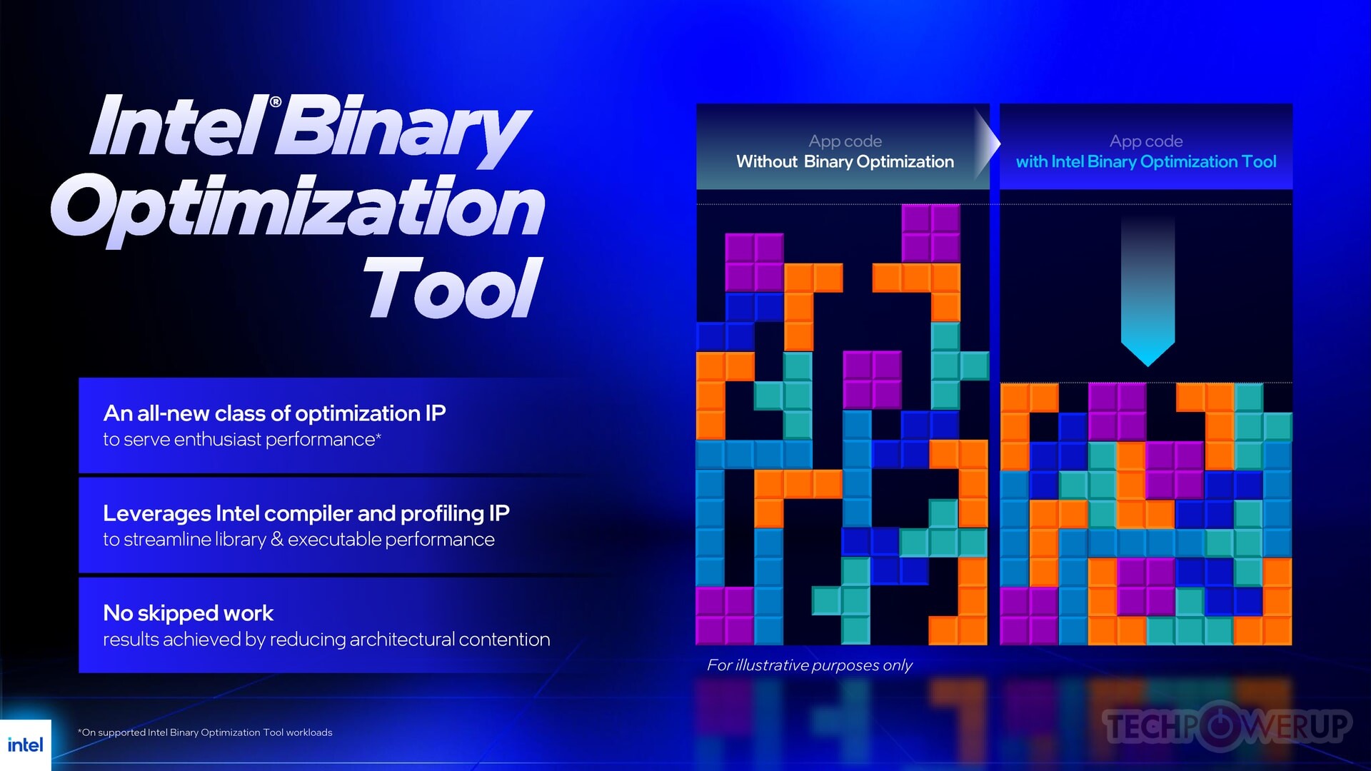
Intel Binary Optimization Technology is the biggest feature announcement with these new processors. This feature allows for a runtime modification of a game's machine code, to better streamline and restructure known function calls by the binary to make better use of Intel's core design, effectively improving IPC, resulting in higher frame-rates from CPU-side performance improvements. Binary Optimization is strictly application-specific, and Intel works diligently with game developers to release application profiles for games with each new IPPP release. This is crucial to prevent Binary Optimization—specifically its runtime code modification—from unintentionally triggering anti-cheat or DRM safeguards.
To create application profiles for Binary Optimization, Intel uses its own toolchains, such as the hardware-based profile-guided optimization tool (HWPGO), to understand how a game loads its binaries and libraries. HWPGO gives Intel's developers deep insight into how the code is interacting with Intel's architecture design, right from the way core compute resources are utilized, so how worker threads are distributed among cores, to how data moves along the cache hierarchy. Intel then identifies hurdles to performance such as branch mispredictions, cache misses, spinlocks, and intra-core architecture hotspots (for example: suboptimal utilization of INT and FP machinery).
This information is then used by Intel to create profiles specific to the application. The profiles tell Binary Optimization Tool to perform "post-link optimization," to virtually redirect slower machine code to more optimal machine code developed by Intel through the above process. The actual user binary is not edited or tampered with on disk in any way, only the way the code moves from the application to the OS then onto hardware is modified. Think of this as similar to pixel shader replacements for graphics. The best part? The entire Binary Optimization process happens within userland (ring-3), no privilege elevation or direct hardware access are required. Intel does not perform any reverse-engineering or access any source code of the game binaries during the Binary Optimization profile development process.
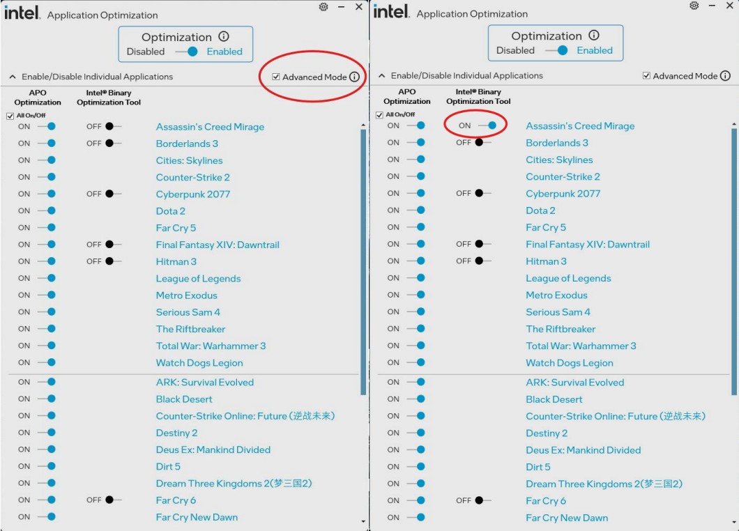
Binary Optimization Tool is a user-facing application that serves as a front-end for the Binary Optimization service, which is built on top of APO. The tool lets you enable or disable Binary Optimization specific to the games installed on your machine. Since this feature is purely opt-in, by default, Binary Optimization is disabled even for known games, for which Intel releases profiles through IPPP. You are expected to launch the Binary Optimization Tool and manually enable it for your game.
Intel 200S Boost Baked Into the Processor
Intel Arrow Lake is a disaggregated, tile-based processor, the various tiles communicate with each other over die-to-die interconnect. Within the Compute tile, the eight P-cores, four E-core clusters, and 36 MB L3 cache, are interconnected using a ringbus. Within the SoC tile, the various bandwidth-heavy components, such as the memory controllers, PCIe root complex, NPU, and media engines, are interconnected using a high-bandwidth switching fabric. Both the die-to-die interconnect (D2D) and SoC tile fabric, have their own clock domains that bear on their data bandwidth.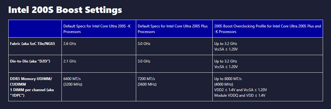
Intel's first wave of Core Ultra Series 2 Arrow Lake-S desktop processors launched in 2024 with a D2D clock speed of 2.10 GHz, and SoC fabric clock of 2.60 GHz. Later down the line in 2025, Intel realized that it could improve performance, particularly in gaming workloads, by increasing these two clock speeds. So it worked with motherboard vendors to release a UEFI BIOS option called "Intel 200S Boost," which increased both the D2D and SoC Fabric clock to 3.20 GHz, without breaking the processor's warranty. The 200S Plus processors come with the D2D clock set to 3.0 GHz out of the box, enabling 200S Boost is still possible and pushes the D2D to 3.2 GHz.
Arrow Lake Architecture
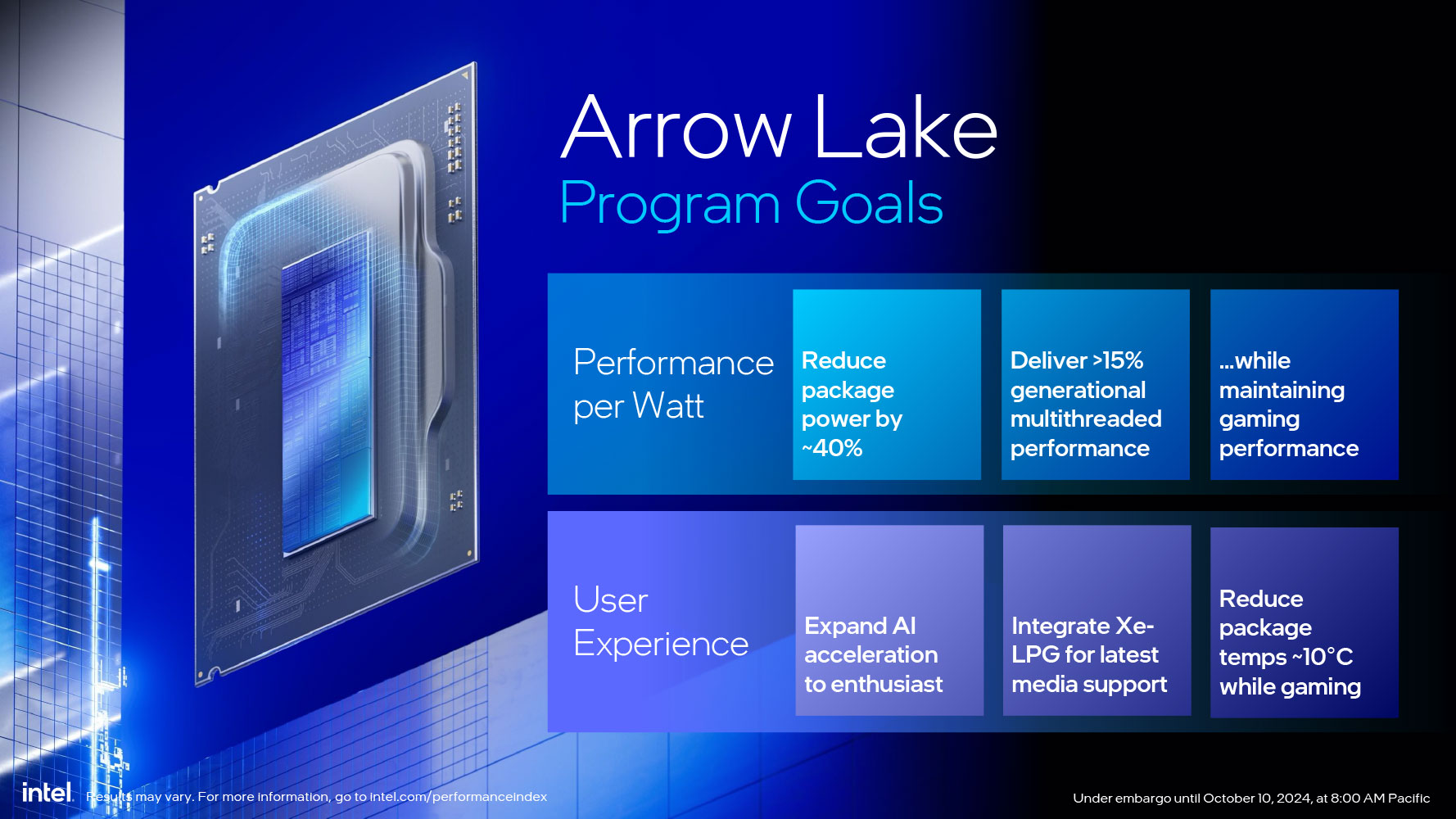
Intel Arrow Lake microarchitecture seeks to advance all key IP blocks of the processor—the CPU cores, the iGPU and platform I/O interfaces, as well as introduce an NPU; but with Intel's pivot to the latest TSMC 3 nm process (something even Apple's latest SoCs are on), there is a concerted effort to offer a leap in energy efficiency and thermals compared to Raptor Lake, which was built on 10 nm (how's that for a leap?). Of course, it's mighty expensive to build a large monolithic die on 3 nm, so Intel implemented its second engineering pivot—to disaggregated tile-based processors arranged on an active interposer. Intel made this pivot on mobile with Meteor Lake and server with Sapphire Rapids, but in 2024 with the launch of Arrow Lake, it arrived at the desktop.
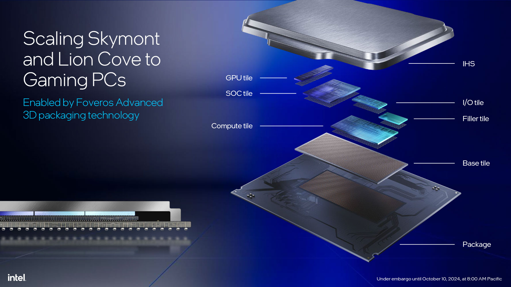
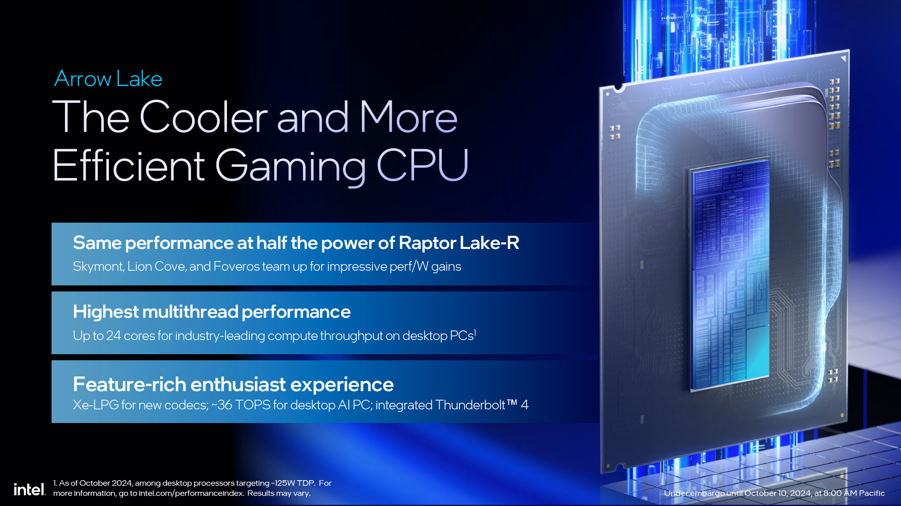
The CPU cores are located on a piece of silicon built on 3 nm, called the Compute tile. This talks to the SoC tile with the memory controllers and PCIe root, and can make do with TSMC 6 nm (the same node AMD uses for its I/O die). This SoC tile also includes Intel's NPU 3. The iGPU is located on a dedicated Graphics tile, which is built on a fairly advanced 5 nm process. All the tiles sit on a Foveros base-tile, which acts like an interposer, facilitating high-density microscopic connections among the tiles, and their connections to the fiberglass substrate below using through-silicon vias. Intel says that the die-area of Arrow Lake-S (8P+16E) is 243 mm², and its total transistor count is 17.8 billion.
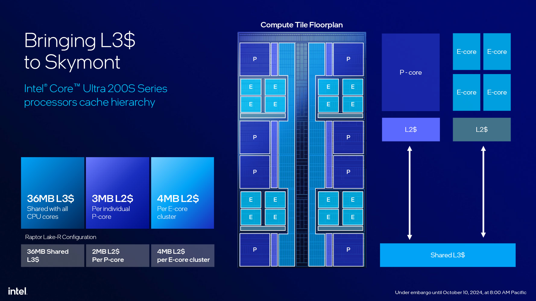
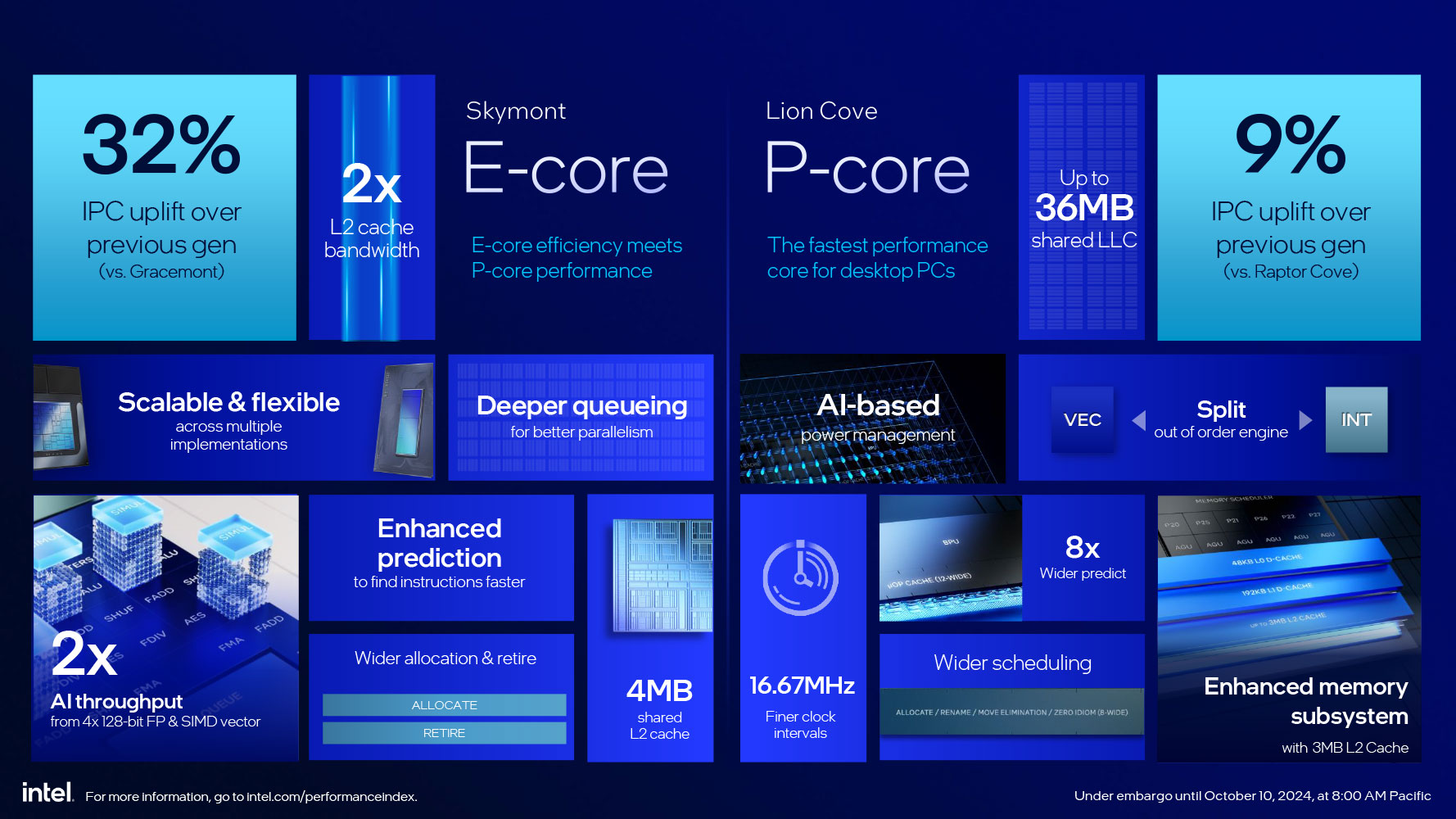
The Compute tile is the most important tile on the processor, it is dedicated to the CPU complex—the collective of 8 Lion Cove performance cores, and 16 Skymont E-cores. All 24 cores share a ringbus interconnect, and a 36 MB L3 cache. Each of the 8 P-cores has a 3 MB L2 cache, the E-cores are arranged in groups of 4 cores, called clusters. Each cluster shares a 4 MB L2 cache among its four cores. Unlike with Alder Lake and Raptor Lake, the P-cores and E-core clusters aren't segregated along two ends of the CPU, rather, they are arranged in alternating rows. There is a row of P-cores, followed by a row of two E-core clusters, and then two rows of P-cores, followed by another row of E-core clusters, and then the final row of P-cores. This approach has two benefits. Firstly, it reduces the concentration of heat during P-core intensive workloads such as gaming. Secondly, it could improve intercore latencies when threads are migrating between P-cores and E-cores, as it cuts down the ringbus stops between the two core types.
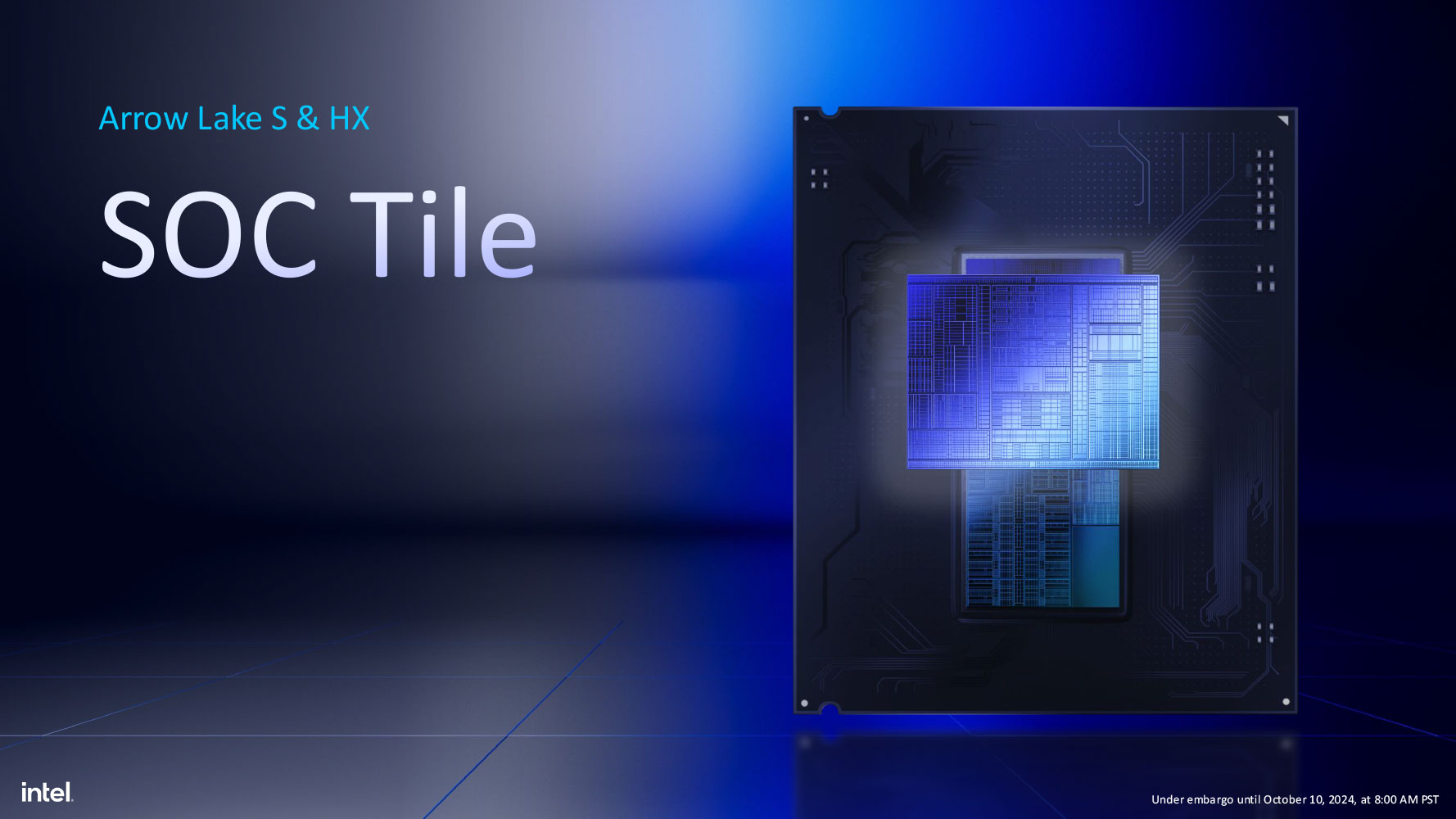
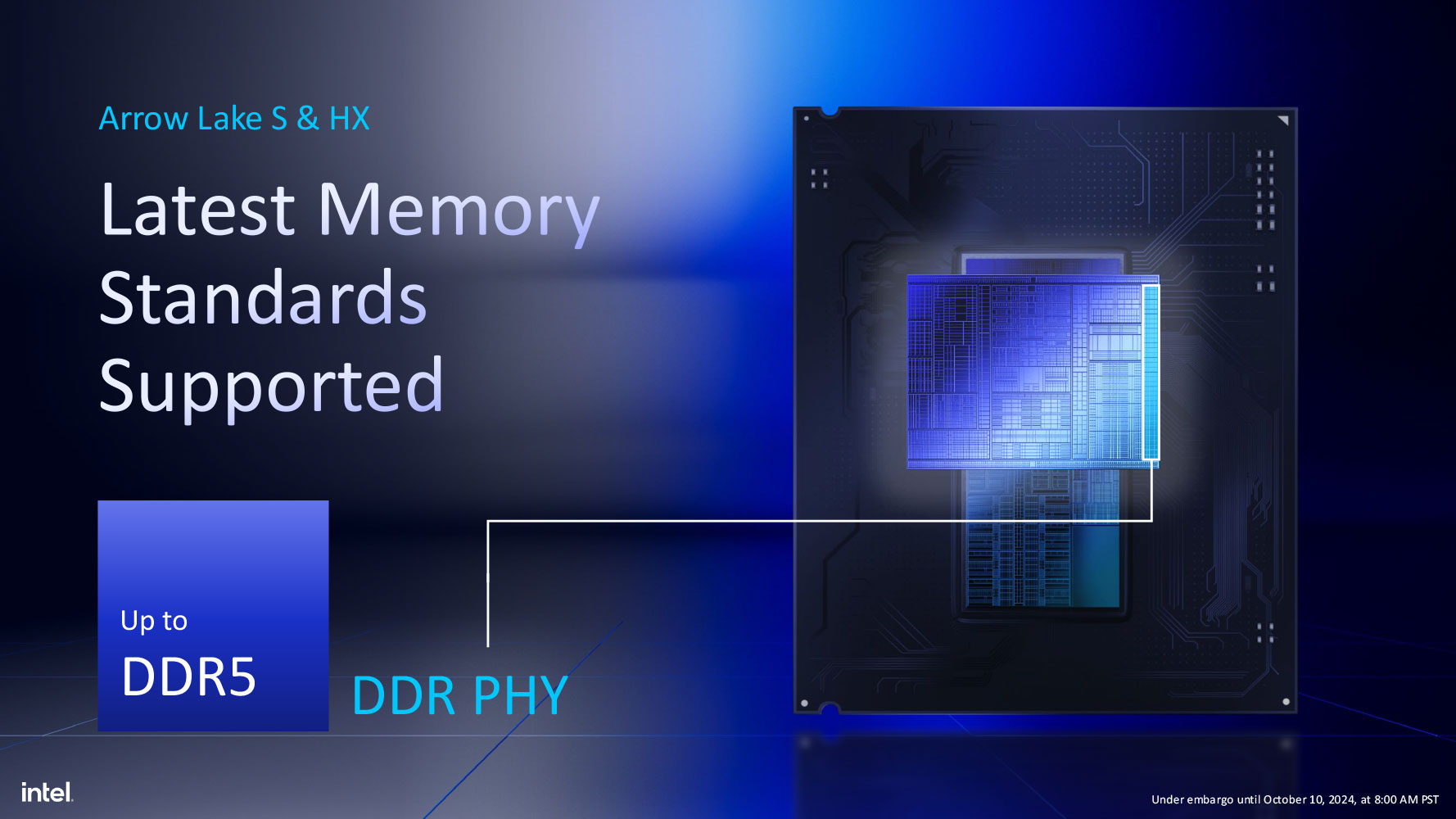
The SoC tile is the next most important tile. This takes up a mostly-central region of the chip, and is built on the 6 nm process. There are no low-power island E-cores on this tile, unlike with "Meteor Lake." The only logic heavy component is the NPU. This tile contains the dual-channel DDR5 memory controller, the DDR5 memory PHY, and the processor's PCI-Express root complex.
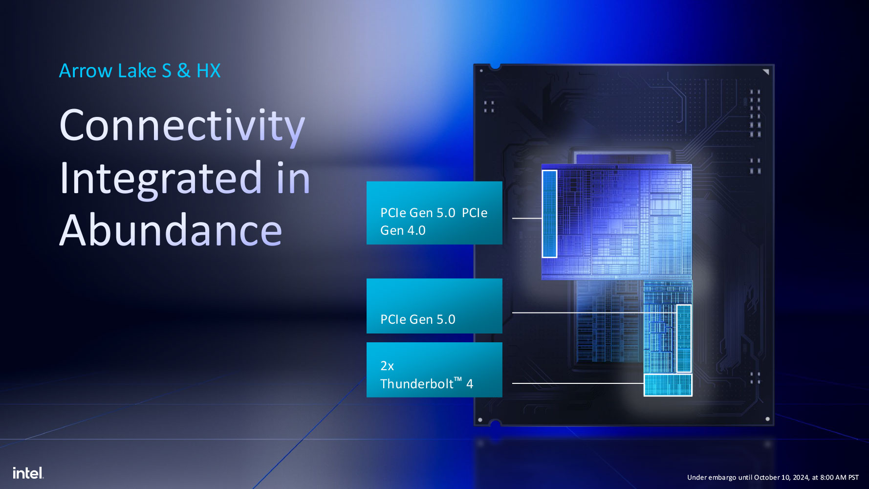
Not counting the DMI 4.0 x8 chipset bus, the processor puts out 20 PCIe Gen 5 lanes. Of these, 16 are dedicated to the PEG interface (for discrete graphics), and four to a dedicated CPU-attached M.2 NVMe slot. There are actually two CPU-attached M.2 slots. Besides the Gen 5 x4, there is a second Gen 4 x4 connection from the processor. This one comes from the breakout I/O tile, which also contains an integrated 40 Gbps Thunderbolt 4 controller. The SoC tile also contains three of the iGPU's allied components, the Display Engine, the Media Acceleration engine, and the Display I/O.
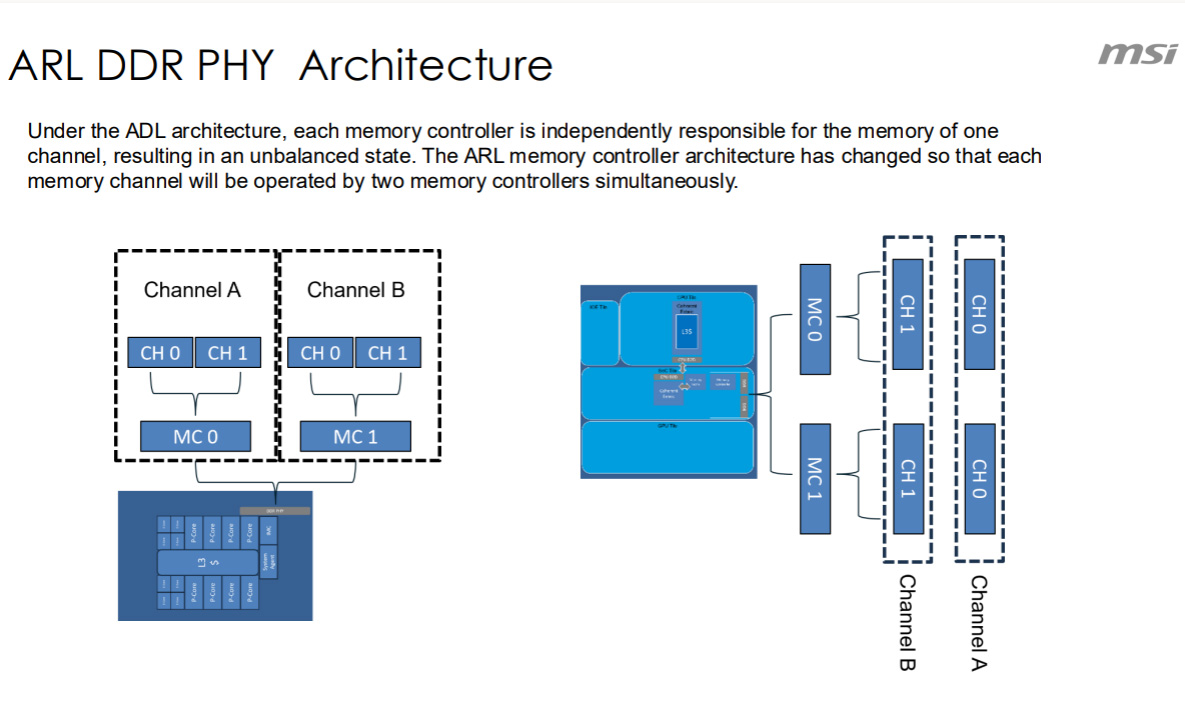
Intel deploys its second generation DDR5 memory controller architecture with Arrow Lake, retiring DDR4 memory support. The older Alder Lake and Raptor Lake generations both feature a memory controller design with two controllers, each handling one channel, and both its 40-bit wide sub-channels; or in DDR4 mode, one controller per memory channel. Since Intel retired DDR4 support, the new architecture sees each of the two memory controllers address a sub-channel of a different channel. So controller 1 would address sub-channels 1 of both channels, while controller 2 would address sub-channels 2 of both channels. This approach probably lets Intel better utilize the sub-channel parallelism on DDR5.
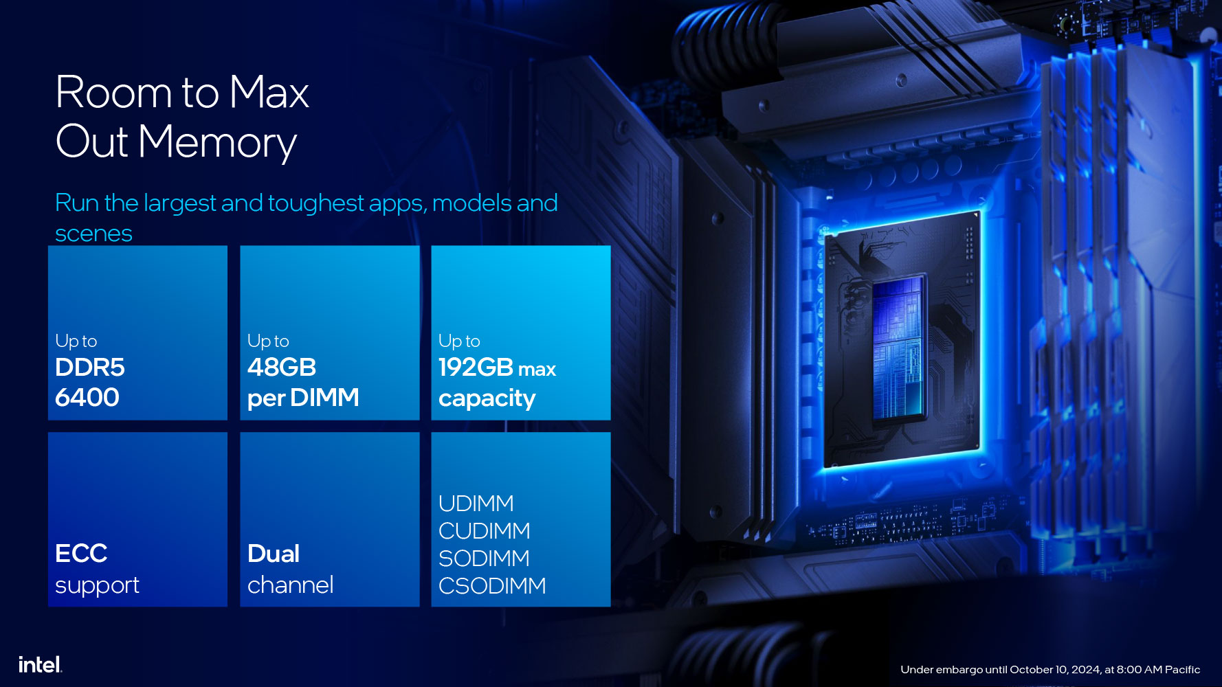
The Plus refresh of Arrow Lake-S supports up to 192 GB of dual-channel memory, with up to 48 GB density per DIMM. It comes with native support for JEDEC DDR5-7200, and Intel says that DDR5-8000 is the "sweetspot" overclocking memory speed. The processors also support overclocked memory speeds well beyond this. There are already announcements of DDR5-9600, and throughout 2026 we should see memory speeds well beyond 10000 MT/s, using memory modules that use CKD chips (CUDIMMs or CSODIMMs). ECC is supported by the architecture, though not on the Z890 chipset, nor by the processor models being announced today.
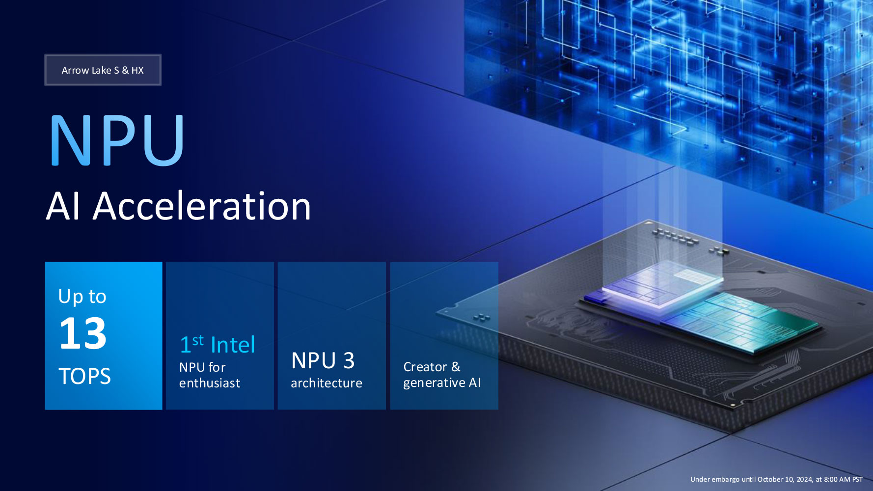
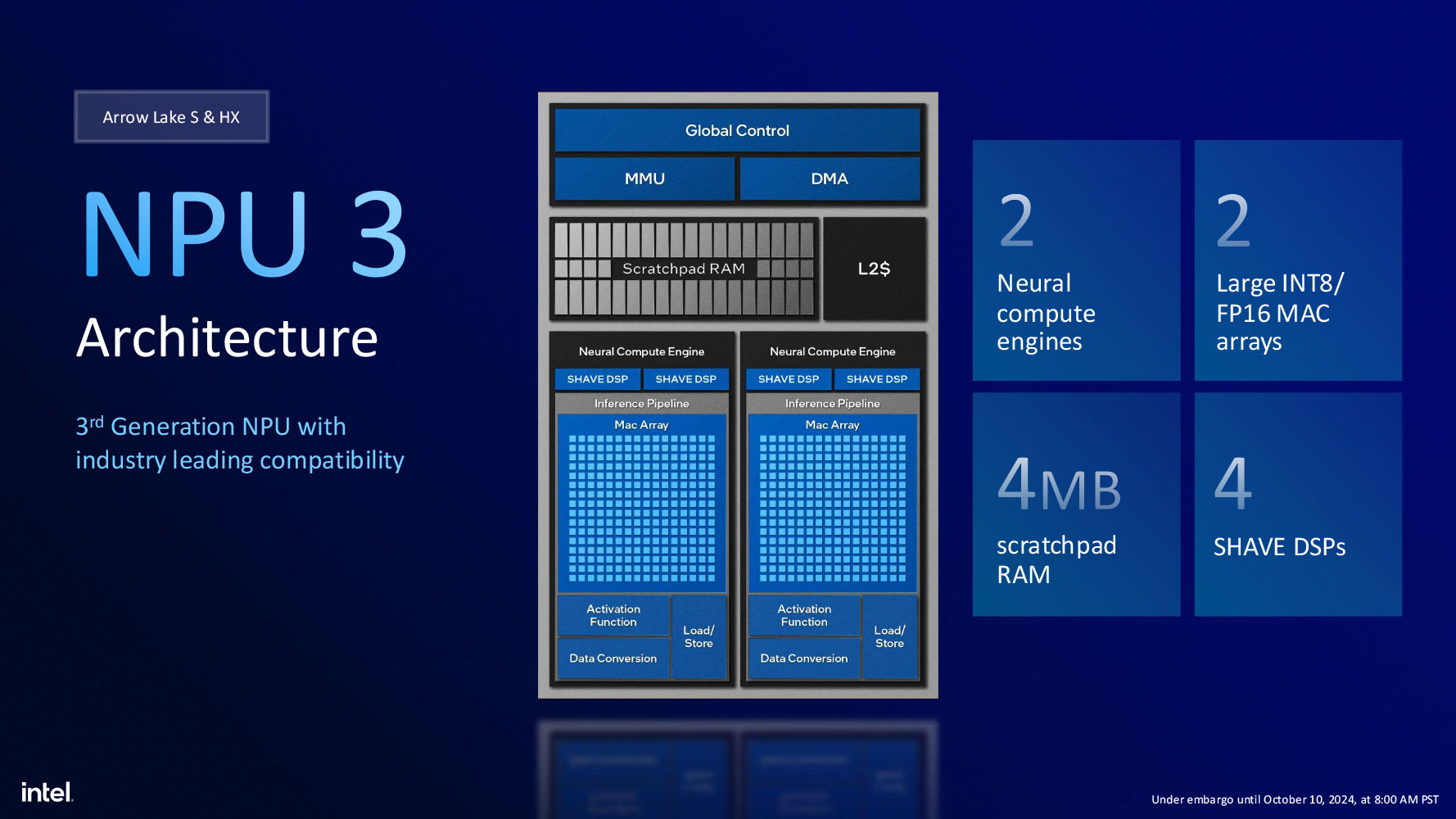
The SoC tile integrates an NPU 3 unit, which appears to have been carried over from "Meteor Lake." This is based on Intel's 3rd Gen NPU architecture, compared to the 4th Gen NPU on "Lunar Lake," and 5th Gen NPU on "Panther Lake." NPU 3 has a peak throughput of 13 AI TOPS, which means it falls short of the 40 TOPS requirement for Microsoft Copilot+ local acceleration. The unit contains two NCEs (neural compute engines), with two INT8/FP16 MAC arrays, four SHAVE DSPs, and a 4 MB scratchpad RAM.
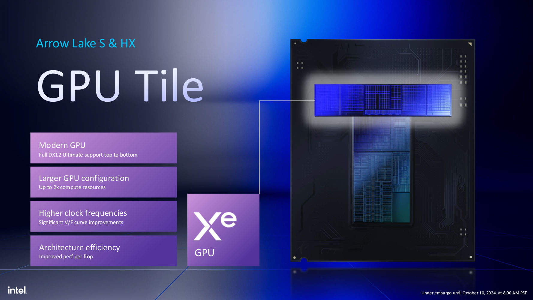
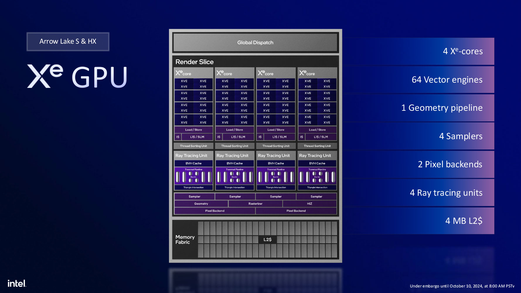
The third key tile of "Arrow Lake" is the Graphics tile, built on the Xe-LPG graphics architecture, which, interestingly, is a generation older than the Xe2 architecture powering the iGPU of "Lunar Lake." The Graphics tile is built on the 5 nm TSMC N5P node. This Graphics tile only contains the iGPU's number crunching and graphics rendering machinery, in the form of a single Xe Rendering Slice with four Xe cores, worth 64 execution units (EUs) or 512 unified shaders. The Xe cores of Arrow Lake's graphics tile lack XMX units. Any AI acceleration is in the form of DP4a, and not XMX. The enthusiast mobile "Arrow Lake-HX" uses the same Graphics tile. On the other hand, "Arrow Lake-H" comes with a larger Graphics tile with eight Xe cores (128 EU, 1,024 unified shaders), and the Xe cores there feature XMX units. Despite having just 4 Xe cores, the Graphics tiles of "Arrow Lake-S" and "Arrow Lake-HX" feature ray tracing units, one per Xe core, which give them full DirectX 12 Ultimate capability. Intel has also given the iGPU a rather large 4 MB L2 cache, which cushions transfers between it and the SoC tile.
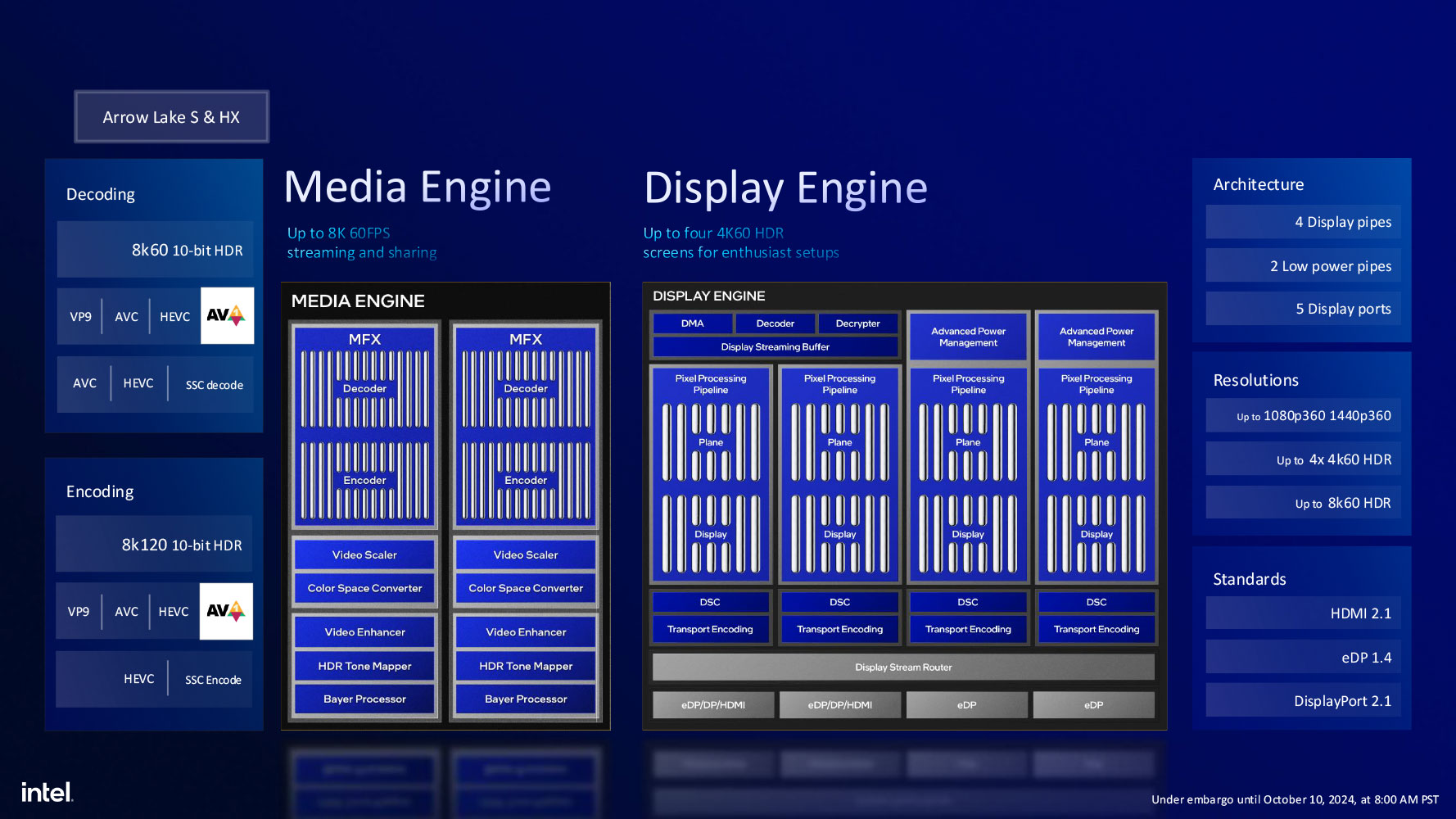
The Media Engine of "Arrow Lake-S" provides hardware-acceleration for video of up to 8K @ 60 Hz with 10-bit HDR, with supported formats that include VP9, AVC, HEVC, AV1, and SSC. Hardware-accelerated encoding is supported for resolutions of up to 8K @ 120 Hz with 10-bit HDR, with supported formats that include VP9, AVC, HEVC, and AV1. The Display Engine supports up to four display pipes with four low-power pipes, and support for up to five display ports. Standards supported include HDMI 2.1, DisplayPort 2.1, and eDP 1.4. Resolutions supported include 8K @ 60 Hz HDR, or four 4K @ 60 Hz HDR, or 1080p @ 360 Hz, or 1440p @ 360 Hz.
Nov 22nd, 2026 10:45 CST
change timezone
Latest GPU Drivers
New Forum Posts
- The TPU UK Clubhouse (27291)
- Can you guess Which game it is? (346)
- Honestly, do you care about GTA VI? (249)
- Your PC ATM (36451)
- Making a game in Godot engine (17)
- TPU's Nostalgic Hardware Club (22197)
- Ryzen or Intel system (20)
- Intel D270 (1)
- Gigabyte AORUS RTX 5080 MASTER – Up to 30°C GPU Hotspot Delta! Is This Normal, a Cooling Defect, or Should I RMA? (14)
- How to prevent OLED burn damage due to PC freezes or power outtages? (55)
Popular Reviews
- Microsoft Surface Laptop Ultra Review - The Next-gen Arm Laptop
- Corsair RM1200e (Second Generation) Review
- Pulsar Office Tour & First Look at P1 Dual-Sensor Mouse
- Upcoming Hardware Launches 2027 (Updated Nov 2026)
- Ugreen NASync DXP4800 GT Review
- AMD Ryzen 7 9800X3D Review - The Best Gaming Processor
- Biwin Black Opal NV7400 2 TB Review
- AMD Zen 6 Technical Deep Dive
- Phantom Blade Zero Performance Benchmark Review - 35 GPUs Tested
- AMD Ryzen 7 5800X3D 10th Anniversary Review
TPU on YouTube
Controversial News Posts
- NVIDIA Co-Founder and CEO Jensen Huang Officially Resigns (492)
- Report: Jensen Huang Eyes NVIDIA Comeback (263)
- Open Letter Asking NVIDIA to Reinstate Jensen Huang Passes 115,000 Signatures (184)
- OpenAI CEO Argues Home PCs Waste the World's Limited DRAM Supply (152)
- NVIDIA Launches Investigation Into Jensen Huang's Relationship With Suspected Chinese Spy (136)
- Intel "Raptor Lake Next" 16-Core and 20-Core CPUs Surface (130)
- NVIDIA GeForce RTX 50-Series Scheduled for up to $500 Price Hike This Week (89)
- Intel Razor Lake Gets a 12 P-Core bLLC Chip With No E-Cores, Per Leak (86)