 17
17
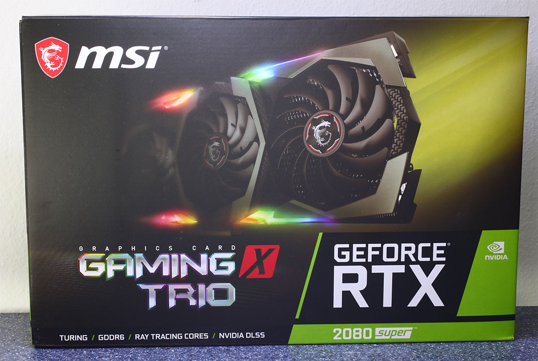
MSI GeForce RTX 2080 Super Gaming X Trio Review
(17 Comments) »Introduction
NVIDIA's GeForce RTX 20 Super series launch in two phases across July is topped off by the new GeForce RTX 2080 Super. Designed to displace the RTX 2080 from the company's product stack at $700, the RTX 2080 Super not just maxes out the 12 nm "TU104" Turing silicon, but also comes with higher GPU clock speeds and faster 15.5 Gbps GDDR6 memory. NVIDIA's reason to launch the RTX 2080 Super may have been necessitated by, of all things, the $399 Radeon RX 5700 XT.
AMD's Radeon RX 5700-series "Navi" launch destabilized NVIDIA's lineup. The RX 5700 XT outperformed the RTX 2070, and the RX 5700 beat the RTX 2060, forcing NVIDIA to launch the RTX 2060 Super and RTX 2070 Super to recapture the $399 and $499 price points. This had a ripple effect on the RTX 2080 because the RTX 2070 Super was carved out from the same "TU104" silicon and since the original RTX 2070 maxed out the "TU106." The RTX 2070 Super performs within 6-8 percent of the RTX 2080 while being $200 cheaper. Custom-design, factory-overclocked RTX 2070 Super cards narrow the performance gap to as little as 3-4 percent. NVIDIA would need to refresh the RTX 2080 lest it gets cannibalized by the RTX 2070 Super. We hence have the new RTX 2080 Super.

NVIDIA's objectives with the RTX 2080 Super are to increase the performance gap with the RTX 2070 Super, so it can justify selling it at a $200 premium, at $700 and avoid tapping into the larger "TU102" silicon, which would escalate costs. The company's approach hence is to supercharge the "TU104". For starters, all 3,072 CUDA cores physically present on the chip are enabled. The original RTX 2080 only features 2,944 of them. Secondly, the GPU Boost frequency is dialed up by a further 100 MHz, to 1815 MHz (up 6 percent). Lastly, the company increased the memory bandwidth by 11 percent by dialing memory clock speeds up to 15.5 Gbps using fast 16 Gbps-rated memory chips.
NVIDIA is also allowing its add-in card (AIC) partners to innovate custom-design RTX 2080 Super graphics cards with generous factory-overclocked speeds and meaty cooling solutions. With prices starting at $700, NVIDIA partners have $200 to mark up prices of their premium offerings because beyond $900, you should aim for the RTX 2080 Ti.
In this review, we have with us the MSI GeForce RTX 2080 Super Gaming X Trio. The card is based on the same "Gaming X Trio" board design as both the RTX 2070 Super and RTX 2080 cards with the name. The card uses a strong 10+2 phase VRM and the humongous Tri Frozr cooling solution that mates a multi fin-stack heatsink with three independently controllable fans and idle fan stop. The card also ships with a 1845 MHz boost frequency, while the memory is left untouched at 15.5 Gbps. MSI is pricing the card at $740, which is a $40 premium over the $700 MSRP for the RTX 2080 Super.
| Price | Shader Units | ROPs | Core Clock | Boost Clock | Memory Clock | GPU | Transistors | Memory | |
|---|---|---|---|---|---|---|---|---|---|
| RX Vega 64 | $400 | 4096 | 64 | 1247 MHz | 1546 MHz | 953 MHz | Vega 10 | 12500M | 8 GB, HBM2, 2048-bit |
| GTX 1080 Ti | $700 | 3584 | 88 | 1481 MHz | 1582 MHz | 1376 MHz | GP102 | 12000M | 11 GB, GDDR5X, 352-bit |
| RX 5700 XT | $400 | 2560 | 64 | 1605 MHz | 1755 MHz | 1750 MHz | Navi 10 | 10300M | 8 GB, GDDR6, 256-bit |
| RTX 2070 | $440 | 2304 | 64 | 1410 MHz | 1620 MHz | 1750 MHz | TU106 | 10800M | 8 GB, GDDR6, 256-bit |
| RTX 2070 Super | $500 | 2560 | 64 | 1605 MHz | 1770 MHz | 1750 MHz | TU104 | 13600M | 8 GB, GDDR6, 256-bit |
| Radeon VII | $680 | 3840 | 64 | 1802 MHz | N/A | 1000 MHz | Vega 20 | 13230M | 16 GB, HBM2, 4096-bit |
| RTX 2080 | $630 | 2944 | 64 | 1515 MHz | 1710 MHz | 1750 MHz | TU104 | 13600M | 8 GB, GDDR6, 256-bit |
| RTX 2080 Super | $700 | 3072 | 64 | 1650 MHz | 1815 MHz | 1940 MHz | TU104 | 13600M | 8 GB, GDDR6, 256-bit |
| MSI RTX 2080 Super Gaming X Trio | $780 | 3072 | 64 | 1650 MHz | 1845 MHz | 1940 MHz | TU104 | 13600M | 8 GB, GDDR6, 256-bit |
| RTX 2080 Ti | $1100 | 4352 | 64 | 1350 MHz | 1545 MHz | 1750 MHz | TU102 | 18600M | 11 GB, GDDR6, 352-bit |
Packaging and Contents

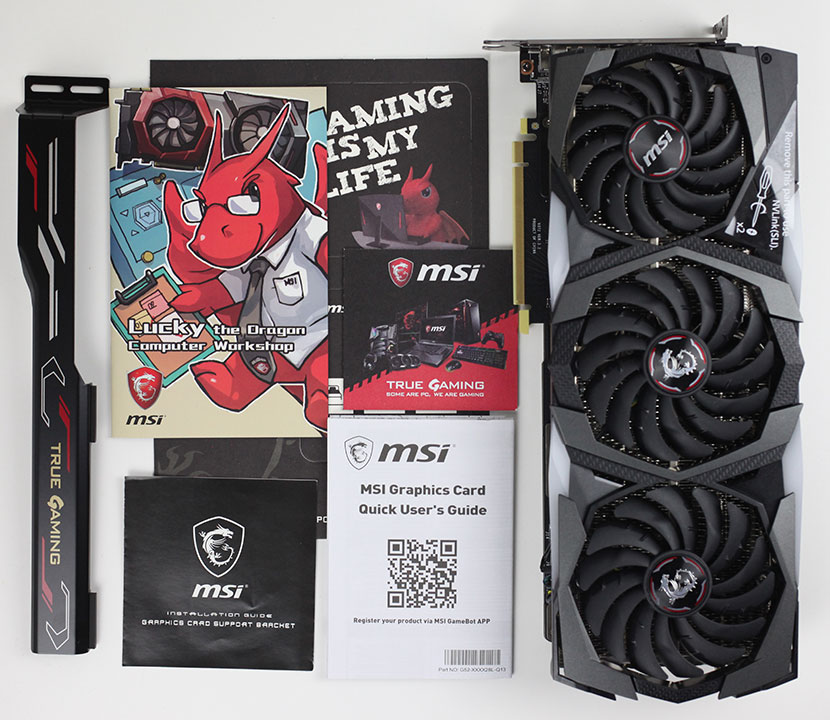
You will receive:
- Graphics card
- Documentation
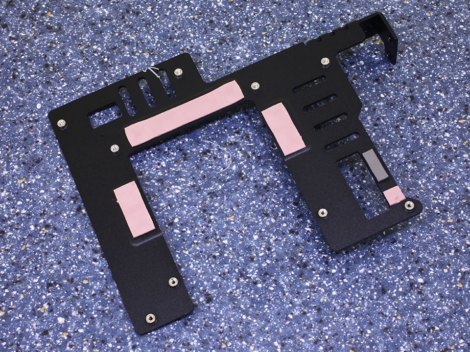
- Anti-sag reinforcement brace
The Card
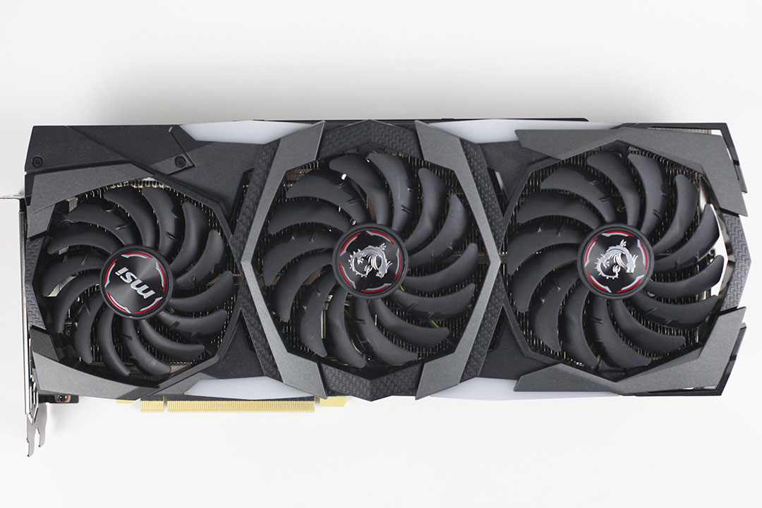

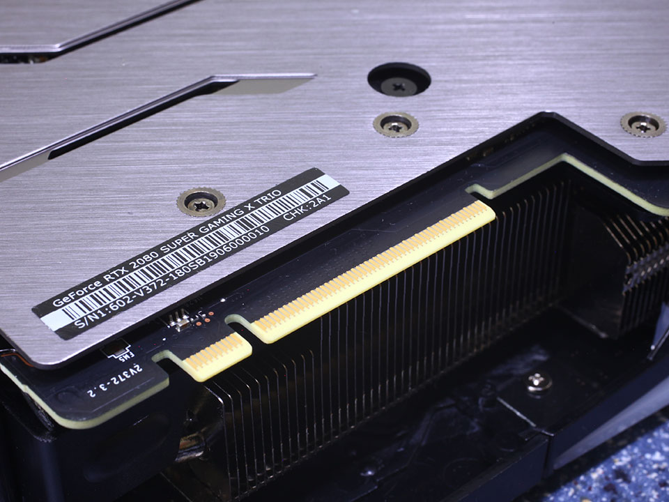
The MSI RTX 2080 Super Gaming X Trio looks identical to the RTX 2080 Gaming X Trio, which of course makes economical sense. On the back, you'll find a high-quality metal backplate. Dimensions of the card are 33x14 cm.
Installation requires three slots in your system.

Display connectivity options include three standard DisplayPort 1.4a, one HDMI 2.0b, and a VirtualLink connector, which is basically USB-C with DisplayPort routing and USB-PD, so a single cable can power, display, and take input from your VR HMD.
NVIDIA has updated their display engine with the Turing microarchitecture, which now supports DisplayPort 1.4a with support for VESA's nearly lossless Display Stream Compression (DSC). Combined, this enables support for 8K@30Hz with a single cable or 8K@60Hz when DSC is turned on. For context, DisplayPort 1.4a is the latest version of the standard that was published in April, 2018.
At CES 2019, NVIDIA announced that all their graphics cards will now support VESA Adaptive Sync (aka FreeSync). While only a small number of FreeSync monitors have been fully qualified with G-SYNC, users can enable the feature in NVIDIA's control panel regardless of whether the monitor is certified or not.
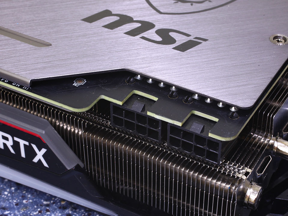
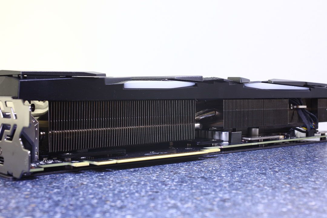
The board uses two 8-pin power connectors. This input configuration is specified for up to 375 watts of power draw.
With Turing, NVIDIA is using NVLink as a physical layer for its next-generation SLI technology. NVLink provides sufficient bandwidth for multi-GPU rendering at 8K 60 Hz, 4K 120 Hz, and other such bandwidth-heavy display resolutions. It's a point-to-point link between your GPUs, so latencies will be lower compared to pushing data through the PCI-Express bus.
Disassembly
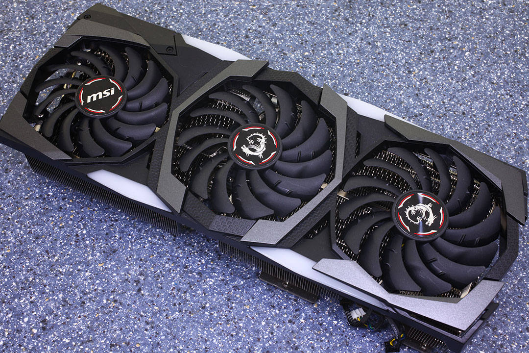

MSI is using a complex dual aluminium fin-stack cooler design that draws heat from the GPU through seven heat pipes and is ventilated by three fans.


Once the main heatsink is removed, a black baseplate becomes visible, which provides cooling for part of the VRM circuitry and memory chips.
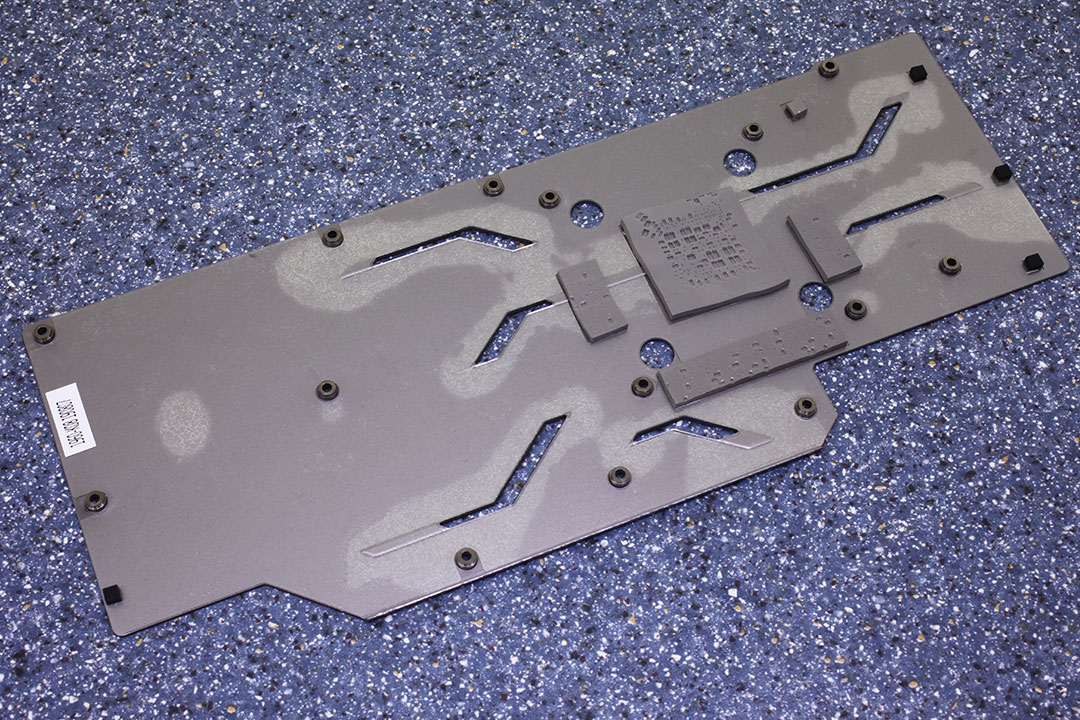

The backplate is made out of metal and protects the card against damage during installation and handling.
On the next page, we dive deep into the PCB layout and VRM configuration.
High-resolution PCB Pictures
These pictures are for the convenience of volt-modders and people who would like to see all the finer details on the PCB. Feel free to link back to us and use them in your articles or forum posts.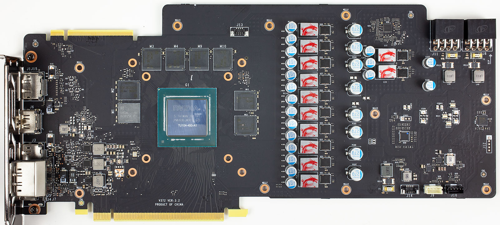
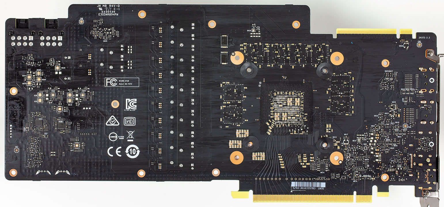
High-res versions are also available (front, back).
Our Patreon Silver Supporters can read articles in single-page format.
Apr 19th, 2024 16:19 EDT
change timezone
Latest GPU Drivers
New Forum Posts
- I9 13890HX undervolting Suggestions (3)
- Linus watercools (50)
- AAF Optimus DCH Audio Modded Driver for Windows 10/11 - For ALL HDAUDIO Enumerator Chips (640)
- I7-8750H + GTX 1050ti Laptop drops performance periodically (3)
- Roccat Kone AIMO has developed a double left click, when I click it once. Any fix out there? (29)
- Share your AIDA 64 cache and memory benchmark here (2882)
- [WIN11] 5700x3d Security processor Attestation: Not supported? (7)
- What are you playing? (20469)
- XFX RX560 1024 shaders 16 CU 4GB from Aliexpress (10)
- DDR5 RAM Speeds and the future (51)
Popular Reviews
- Horizon Forbidden West Performance Benchmark Review - 30 GPUs Tested
- PowerColor Radeon RX 7900 GRE Hellhound Review
- Fractal Design Terra Review
- Corsair 2000D Airflow Review
- Thermalright Phantom Spirit 120 EVO Review
- Minisforum EliteMini UM780 XTX (AMD Ryzen 7 7840HS) Review
- Creative Pebble X Plus Review
- FiiO KB3 HiFi Mechanical Keyboard Review - Integrated DAC/Amp!
- ASUS GeForce RTX 4090 STRIX OC Review
- NVIDIA GeForce RTX 4090 Founders Edition Review - Impressive Performance
Controversial News Posts
- Sony PlayStation 5 Pro Specifications Confirmed, Console Arrives Before Holidays (110)
- NVIDIA Points Intel Raptor Lake CPU Users to Get Help from Intel Amid System Instability Issues (102)
- US Government Wants Nuclear Plants to Offload AI Data Center Expansion (98)
- Windows 10 Security Updates to Cost $61 After 2025, $427 by 2028 (82)
- Developers of Outpost Infinity Siege Recommend Underclocking i9-13900K and i9-14900K for Stability on Machines with RTX 4090 (82)
- AMD "Strix Halo" Zen 5 Mobile Processor Pictured: Chiplet-based, Uses 256-bit LPDDR5X (76)
- TechPowerUp Hiring: Reviewers Wanted for Motherboards, Laptops, Gaming Handhelds and Prebuilt Desktops (72)
- Intel Realizes the Only Way to Save x86 is to Democratize it, Reopens x86 IP Licensing (70)