 63
63
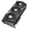
MSI GeForce RTX 3060 Gaming X Trio Review
Test Setup »High-resolution PCB Pictures
These pictures are for the convenience of volt modders and people who would like to see all the finer details on the PCB. Feel free to link back to us and use these in your articles or forum posts.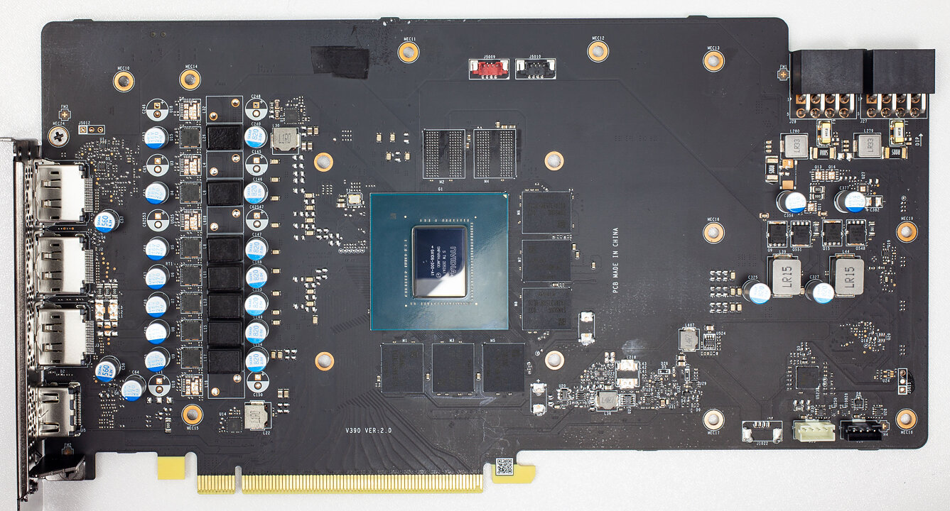

High-res versions are also available (front, back).
Circuit Board (PCB) Analysis
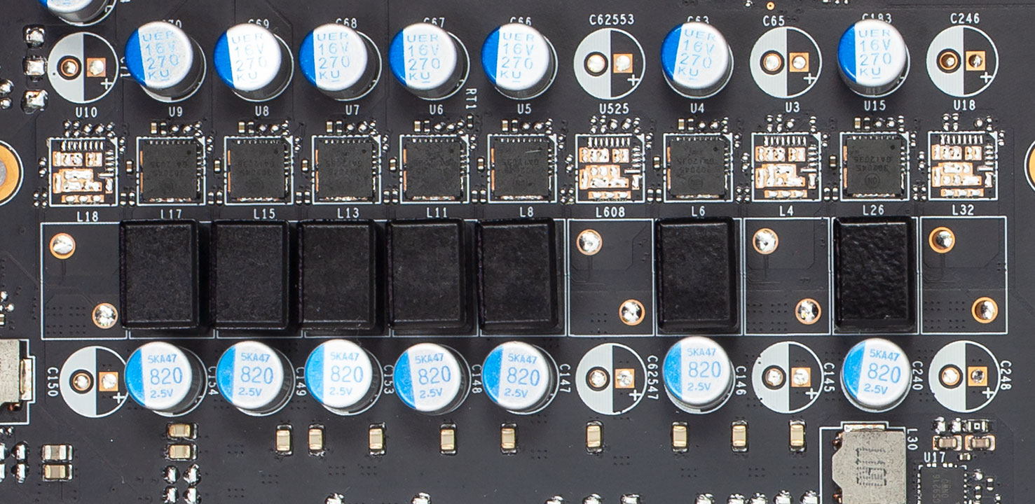

GPU voltage is 7-phase and managed by an OnSemi NCP81610 controller.

The DrMOS for the GPU are OnSemi 302045 chips.


Memory voltage is a two-phase design generated by a 7222 buck controller.

For memory, Niko Semi PK616BA MOSFETs are used.

The GDDR6 chips are made by Samsung, carry the model number "K4ZAF325BM-HC16," and are rated to run at 16 Gbps.
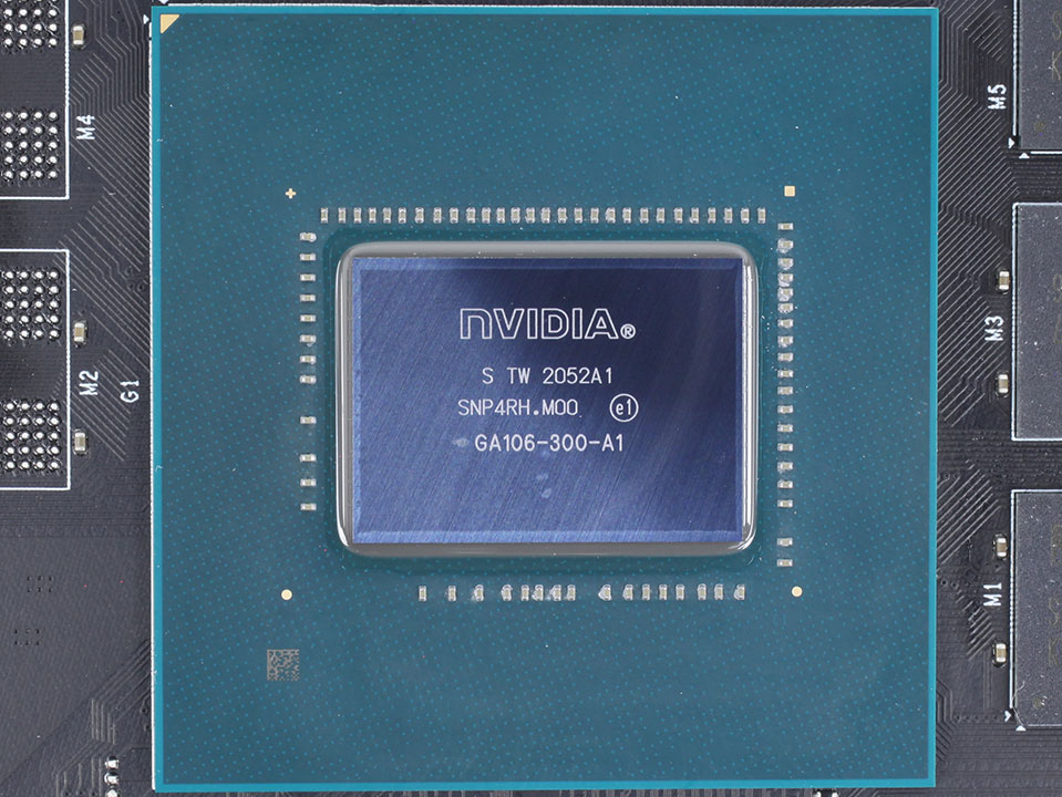
NVIDIA's GA106 graphics processor is the company's third GeForce Ampere architecture chip. It is produced on a 8 nanometer process at Samsung and has a transistor count of 13.3 billion with a die size of 276 mm².
May 5th, 2024 20:41 EDT
change timezone
Latest GPU Drivers
New Forum Posts
- FINAL FANTASY XIV: Dawntrail Official Benchmark (84)
- Only some humans can see refresh rates faster than others, I am one of those humans. (131)
- Apparently Valve is giving refunds on Helldivers 2 regardless of hour count. Details inside. (71)
- The Official Thermal Interface Material thread (1157)
- Random black screen - GPU or PSU bricked? (9)
- Benchmarking Unity graphics performance in WebGL (42)
- Arctic MX-6 shelf life is just a couple months? (92)
- Horizontal black lines popping up on my screen? (15)
- [HELP] AMD GPU FINDING BIOS PROBLEM (11)
- Envinda RX 580 2048SP 8GB no image (13)
Popular Reviews
- Finalmouse UltralightX Review
- ASRock NUC BOX-155H (Intel Core Ultra 7 155H) Review
- Meze Audio LIRIC 2nd Generation Closed-Back Headphones Review
- Cougar Hotrod Royal Gaming Chair Review
- Upcoming Hardware Launches 2023 (Updated Feb 2024)
- Montech Sky Two GX Review
- AMD Ryzen 7 7800X3D Review - The Best Gaming CPU
- HYTE THICC Q60 240 mm AIO Review
- ASUS Radeon RX 7900 GRE TUF OC Review
- Logitech G Pro X Superlight 2 Review - Updated with 4000 Hz Tested
Controversial News Posts
- Intel Statement on Stability Issues: "Motherboard Makers to Blame" (240)
- Windows 11 Now Officially Adware as Microsoft Embeds Ads in the Start Menu (167)
- AMD to Redesign Ray Tracing Hardware on RDNA 4 (153)
- Sony PlayStation 5 Pro Specifications Confirmed, Console Arrives Before Holidays (117)
- AMD's RDNA 4 GPUs Could Stick with 18 Gbps GDDR6 Memory (114)
- NVIDIA Points Intel Raptor Lake CPU Users to Get Help from Intel Amid System Instability Issues (106)
- AMD Ryzen 9 7900X3D Now at a Mouth-watering $329 (104)
- AMD "Strix Halo" Zen 5 Mobile Processor Pictured: Chiplet-based, Uses 256-bit LPDDR5X (103)