 7
7
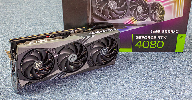
MSI GeForce RTX 4080 Gaming X Trio Review
(7 Comments) »Introduction
MSI GeForce RTX 4080 Gaming X Trio continues on the solid legacy of MSI's award-winning Gaming X line of graphics cards that changed the landscape of custom-design, propelling MSI to being one of the top graphics card vendors. Its design appeals to gamers who want a little more from their RTX 4080 graphics card, in terms of design as well as performance, and like to flaunt their hardware's aesthetics. The new GeForce RTX 4080 "Ada Lovelace" cements NVIDIA's domination in the high-end segment with a second product that does the same things as the RTX 4090—4K Ultra HD maxed-out gaming with ray tracing; at a more appealing starting price of $1,200.
With the GeForce RTX 4080, NVIDIA introduces the new AD103 silicon, which borrows the best of both the high-end AD102, and the performance-segment AD104. The GPU has a high CUDA core count, with 9,728 enabled on the RTX 4080; while having an optimized 256-bit wide GDDR6X memory interface driving 16 GB of memory, more than the 10 GB or 12 GB available to the previous-generation RTX 3080. NVIDIA attempted to overcome the shortfall in memory bandwidth with faster 22.4 Gbps memory, and larger on-die caches that lubricate the memory sub-system.
The RTX 4080 is endowed with 9,728 CUDA cores across 76 streaming multiprocessors, 304 Tensor cores, 76 RT cores, and 112 ROPs. The GPU is normally clocked at 2.50 GHz boost, which MSI has overclocked to 2.59 GHz. The MSI Gaming X cooler features a meaty 3-slot cooling solution with three Axial-Tech fans, and an elaborate RGB LED setup with multiple diffusers. The card draws power from the same 16-pin 12VHPWR connector, but which is keyed for 450 W delivery, as is the included power adapter with three 8-pin PCIe power inputs. MSI is pricing the RTX 4080 Gaming X Trio at $1,310, a $110 premium over the NVIDIA baseline.
| Price | Cores | ROPs | Core Clock | Boost Clock | Memory Clock | GPU | Transistors | Memory | |
|---|---|---|---|---|---|---|---|---|---|
| RTX 2080 | $380 | 2944 | 64 | 1515 MHz | 1710 MHz | 1750 MHz | TU104 | 13600M | 8 GB, GDDR6, 256-bit |
| RTX 3060 Ti | $410 | 4864 | 80 | 1410 MHz | 1665 MHz | 1750 MHz | GA104 | 17400M | 8 GB, GDDR6, 256-bit |
| RX 6700 XT | $360 | 2560 | 64 | 2424 MHz | 2581 MHz | 2000 MHz | Navi 22 | 17200M | 12 GB, GDDR6, 192-bit |
| RX 6750 XT | $470 | 2560 | 64 | 2495 MHz | 2600 MHz | 2250 MHz | Navi 22 | 17200M | 12 GB, GDDR6, 192-bit |
| RTX 2080 Ti | $600 | 4352 | 88 | 1350 MHz | 1545 MHz | 1750 MHz | TU102 | 18600M | 11 GB, GDDR6, 352-bit |
| RTX 3070 | $500 | 5888 | 96 | 1500 MHz | 1725 MHz | 1750 MHz | GA104 | 17400M | 8 GB, GDDR6, 256-bit |
| RTX 3070 Ti | $600 | 6144 | 96 | 1575 MHz | 1770 MHz | 1188 MHz | GA104 | 17400M | 8 GB, GDDR6X, 256-bit |
| RX 6800 | $580 | 3840 | 96 | 1815 MHz | 2105 MHz | 2000 MHz | Navi 21 | 26800M | 16 GB, GDDR6, 256-bit |
| RX 6800 XT | $530 | 4608 | 128 | 2015 MHz | 2250 MHz | 2000 MHz | Navi 21 | 26800M | 16 GB, GDDR6, 256-bit |
| RTX 3080 | $660 | 8704 | 96 | 1440 MHz | 1710 MHz | 1188 MHz | GA102 | 28000M | 10 GB, GDDR6X, 320-bit |
| RTX 3080 Ti | $950 | 10240 | 112 | 1365 MHz | 1665 MHz | 1188 MHz | GA102 | 28000M | 12 GB, GDDR6X, 384-bit |
| RX 6900 XT | $650 | 5120 | 128 | 2015 MHz | 2250 MHz | 2000 MHz | Navi 21 | 26800M | 16 GB, GDDR6, 256-bit |
| RX 6950 XT | $800 | 5120 | 128 | 2100 MHz | 2310 MHz | 2250 MHz | Navi 21 | 26800M | 16 GB, GDDR6, 256-bit |
| RTX 3090 | $900 | 10496 | 112 | 1395 MHz | 1695 MHz | 1219 MHz | GA102 | 28000M | 24 GB, GDDR6X, 384-bit |
| RX 7900 XT | $900 | 5376 | 192 | 2000 MHz | 2400 MHz | 2500 MHz | Navi 31 | 58000M | 20 GB, GDDR6, 320-bit |
| RTX 3090 Ti | $1400 | 10752 | 112 | 1560 MHz | 1950 MHz | 1313 MHz | GA102 | 28000M | 24 GB, GDDR6X, 384-bit |
| RX 7900 XTX | $1000 | 6144 | 192 | 2300 MHz | 2505 MHz | 2500 MHz | Navi 31 | 58000M | 24 GB, GDDR6, 384-bit |
| RTX 4080 | $1200 | 9728 | 112 | 2205 MHz | 2505 MHz | 1400 MHz | AD103 | 45900M | 16 GB, GDDR6X, 256-bit |
| MSI RTX 4080 Gaming X Trio | $1310 | 9728 | 112 | 2205 MHz | 2595 MHz | 1400 MHz | AD103 | 45900M | 16 GB, GDDR6X, 256-bit |
| RTX 4090 | $2400 | 16384 | 176 | 2235 MHz | 2520 MHz | 1313 MHz | AD102 | 76300M | 24 GB, GDDR6X, 384-bit |
Architecture
The Ada graphics architecture heralds the third generation of the NVIDIA RTX technology, an effort toward increasing the realism in game visuals by leveraging real-time ray tracing, without the enormous amount of compute power required to draw purely ray-traced 3D graphics. This is done by blending conventional raster graphics with ray traced elements such as reflections, lighting, and global illumination, to name a few. The 3rd generation of RTX heralds the new higher IPC "Ada" CUDA core, 3rd generation RT core, 4th generation Tensor core, and the new Optical Flow Processor, a component that plays a key role in generating new frames without involving the GPU's main graphics rendering pipeline.


The GeForce Ada graphics architecture driving the RTX 4080 leverages the TSMC 5 nm EUV foundry process to increase transistor counts. At the heart of the RTX 4080 is the new AD103 silicon, which has a reasonably large transistor count of 45.9 billion, which is still nearly 60% higher than that of the previous-generation flagship GA102. The GPU features a PCI-Express 4.0 x16 host interface, and a 256-bit wide GDDR6X memory bus, which on the RTX 4080 wires out to 16 GB of memory. With NVIDIA cancelling the 12 GB variant, this is the only RTX 4080 there is, for now. The Optical Flow Accelerator (OFA) is an independent top-level component. The chip features two NVENC and one NVDEC units in the GeForce RTX 40-series.
The essential component hierarchy is similar to past generations of NVIDIA GPUs. The AD103 silicon features 7 Graphics Processing Clusters (GPCs), each of these has all the SIMD and graphics rendering machinery, and is a small GPU in its own right. Each GPC shares a raster engine (geometry processing components) and two ROP partitions (each with eight ROP units). The GPC of the AD102 contains six Texture Processing Clusters (TPCs), the main number-crunching machinery. Each of these has two Streaming Multiprocessors (SM), and a Polymorph unit. Each SM contains 128 CUDA cores across four partitions. Half of these CUDA cores are pure-FP32; while the other half is capable of FP32 or INT32. The SM retains concurrent FP32+INT32 math processing capability. The SM also contains a 3rd generation RT core, four 4th generation Tensor cores, some cache memory, and four TMUs. There are 12 SM per GPC, so 1,536 CUDA cores, 48 Tensor cores, and 12 RT cores; per GPC. There are seven such GPCs, which add up to 10,240 CUDA cores, 320 TMUs, 320 Tensor Cores, 80 RT cores. Each GPC contributes 16 ROPs, so there are 112 ROPs on the silicon. NVIDIA carved the RTX 4080 out of the AD103 by disabling four SMs.
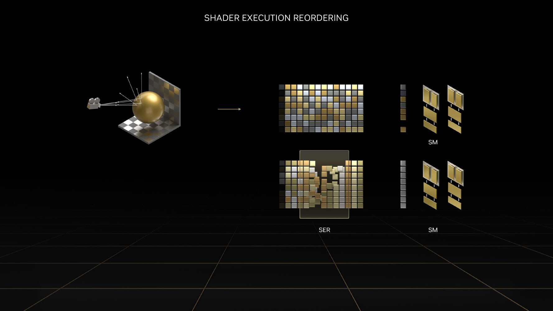

The 3rd generation RT core accelerates the most math-intensive aspects of real-time ray tracing, including BVH traversal. Displaced micro-mesh engine is a revolutionary feature introduced with the new 3rd generation RT core. Just as mesh shaders and tessellation have had a profound impact on improving performance with complex raster geometry, allowing game developers to significantly increase geometric complexity; DMMs is a method to reduce the complexity of the bounding-volume hierarchy (BVH) data-structure, which is used to determine where a ray hits geometry. Previously the BVH had to capture even the smallest details to properly determine the intersection point. Ada's ray tracing architecture receives a major performance uplift from Shader Execution Reordering (SER), a software-defined feature that requires awareness from game-engines, to help the GPU reorganize and optimize worker threads associated with ray tracing.


The BVH now needn't have data for every single triangle on an object, but can represent objects with complex geometry as a coarse mesh of base triangles, which greatly simplifies the BVH data structure. A simpler BVH means less memory consumed and helps to greatly reduce ray tracing CPU load, because the CPU only has to generate a smaller structure. With older "Ampere" and "Turing" RT cores, each triangle on an object had to be sampled at high overhead, so the RT core could precisely calculate ray intersection for each triangle. With Ada, the simpler BVH, plus the displacement maps can be sent to the RT core, which is now able to figure out the exact hit point on its own. NVIDIA has seen 11:1 to 28:1 compression in total triangle counts. This reduces BVH compile times by 7.6x to over 15x, in comparison to the older RT core; and reducing its storage footprint by anywhere between 6.5 to 20 times. DMMs could reduce disk- and memory bandwidth utilization, utilization of the PCIe bus, as well as reduce CPU utilization. NVIDIA worked with Simplygon and Adobe to add DMM support for their tool chains.


Opacity Micro Meshes (OMM) is a new feature introduced with Ada to improve rasterization performance, particularly with objects that have alpha (transparency data). Most low-priority objects in a 3D scene, such as leaves on a tree, are essentially rectangles with textures on the leaves where the transparency (alpha) creates the shape of the leaf. RT cores have a hard time intersecting rays with such objects, because they're not really in the shape that they appear (they're really just rectangles with textures that give you the illusion of shape). Previous-generation RT cores had to have multiple interactions with the rendering stage to figure out the shape of a transparent object, because they couldn't test for alpha by themselves.


This has been solved by using OMMs. Just as DMMs simplify geometry by creating meshes of micro-triangles; OMMs create meshes of rectangular textures that align with parts of the texture that aren't alpha, so the RT core has a better understanding of the geometry of the object, and can correctly calculate ray intersections. This has a significant performance impact on shading performance in non-RT applications, too. Practical applications of OMMs aren't just low-priority objects such as vegetation, but also smoke-sprites and localized fog. Traditionally there was a lot of overdraw for such effects, because they layered multiple textures on top of each other, that all had to be fully processed by the shaders. Now only the non-opaque pixels get executed—OMMs provide a 30 percent speedup with graphics buffer fill-rates, and a 10 percent impact on frame-rates.


DLSS 3 introduces a revolutionary new feature that promises a doubling in frame-rate at comparable quality, it's called AI frame-generation. While it has all the features of DLSS 2 and its AI super-resolution (scaling up a lower-resolution frame to native resolution with minimal quality loss); DLSS 3 can generate entire frames simply using AI, without involving the graphics rendering pipeline. Later in the article, we will show you DLSS 3 in action.


Every alternating frame with DLSS 3 is hence AI-generated, without being a replica of the previous rendered frame. This is possible only on the Ada graphics architecture, because of a hardware component called the optical flow accelerator (OFA), which assists in predicting what the next frame could look like, by creating what NVIDIA calls an optical flow-field. OFA ensures that the DLSS 3 algorithm isn't confused by static objects in a rapidly-changing 3D scene (such as a race sim). The process heavily relies on the performance uplift introduced by the FP8 math format of the 4th generation Tensor core. A third key ingredient of DLSS 3 is Reflex. By reducing the rendering queue to zero, Reflex plays a vital role in ensuring that frame-times with DLSS 3 are at an acceptable level, and a render-queue doesn't confuse the upscaler. A combination of OFA and the 4th Gen Tensor core is why the Ada architecture is required to use DLSS 3, and why it won't work on older architectures.
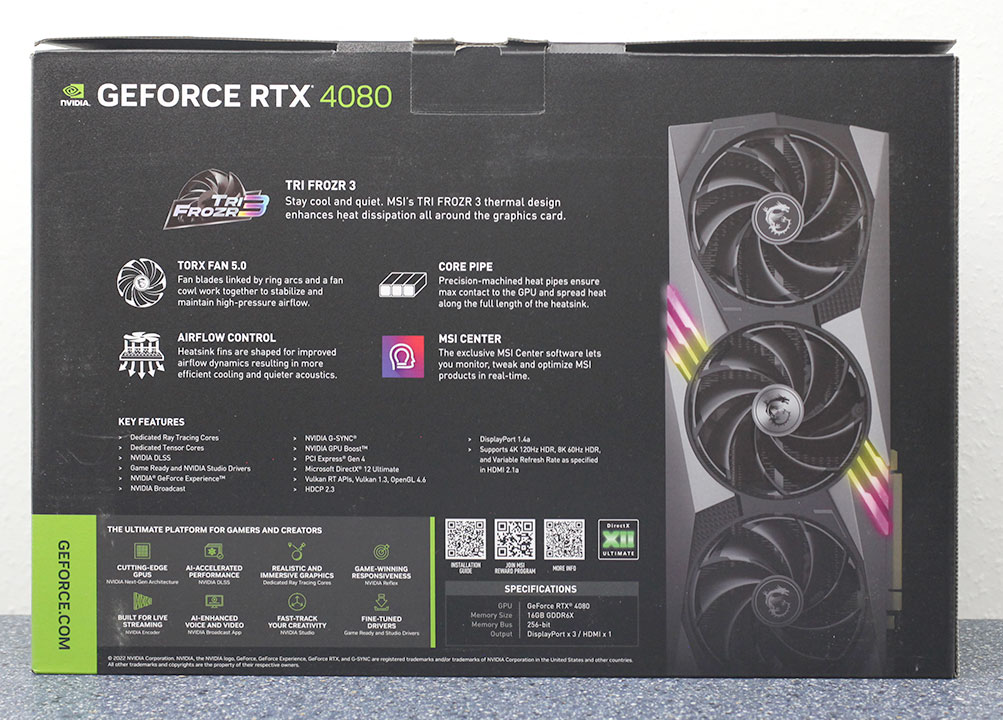
Packaging
The Card
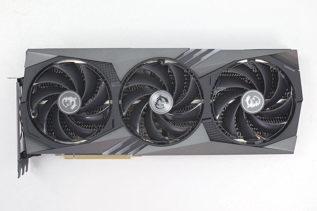
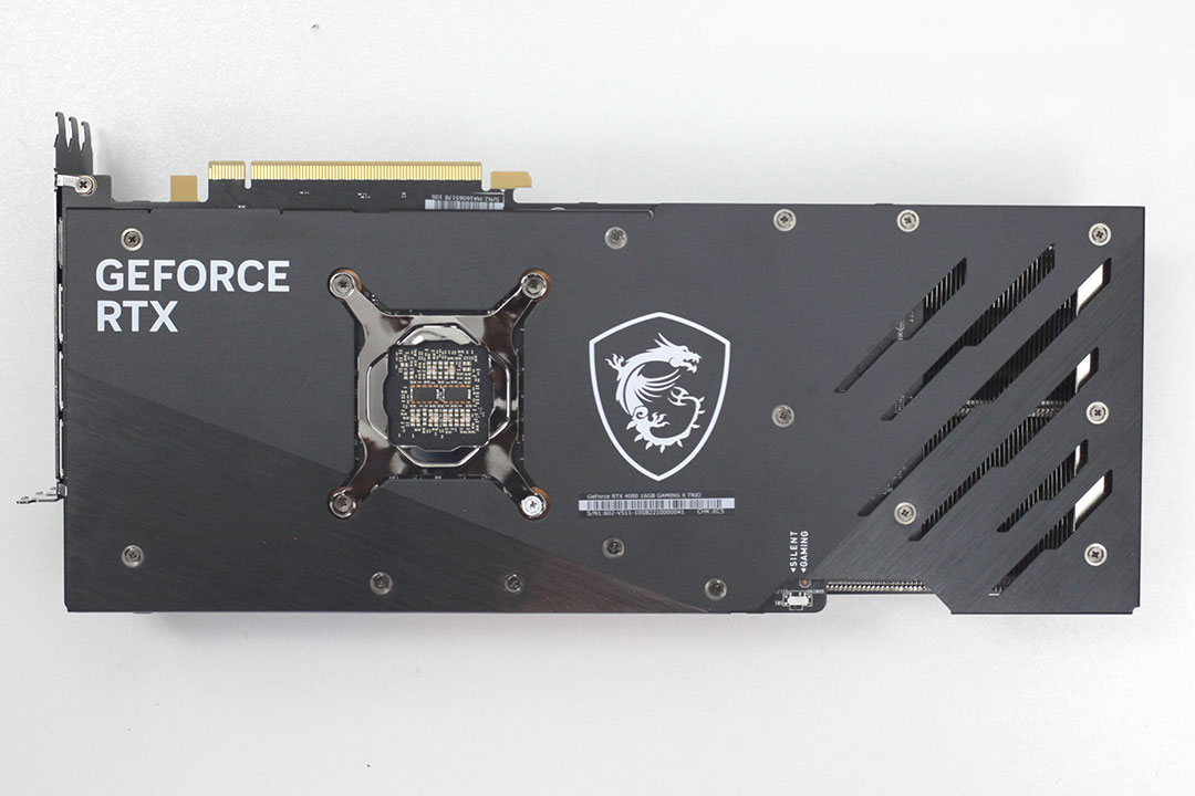
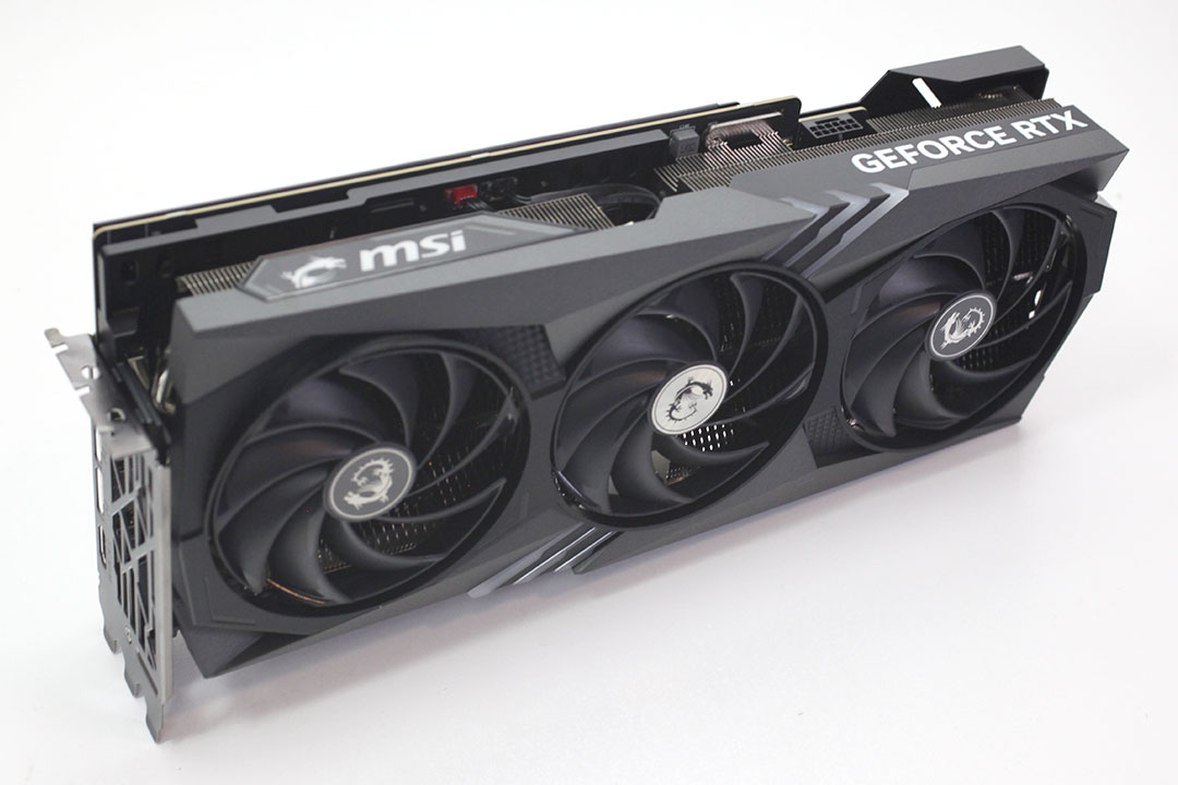
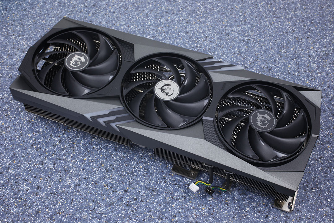
The MSI Gaming X is dominated by black, with various shades of gray as highlights. On the rear you'll find a high-quality metal backplate.
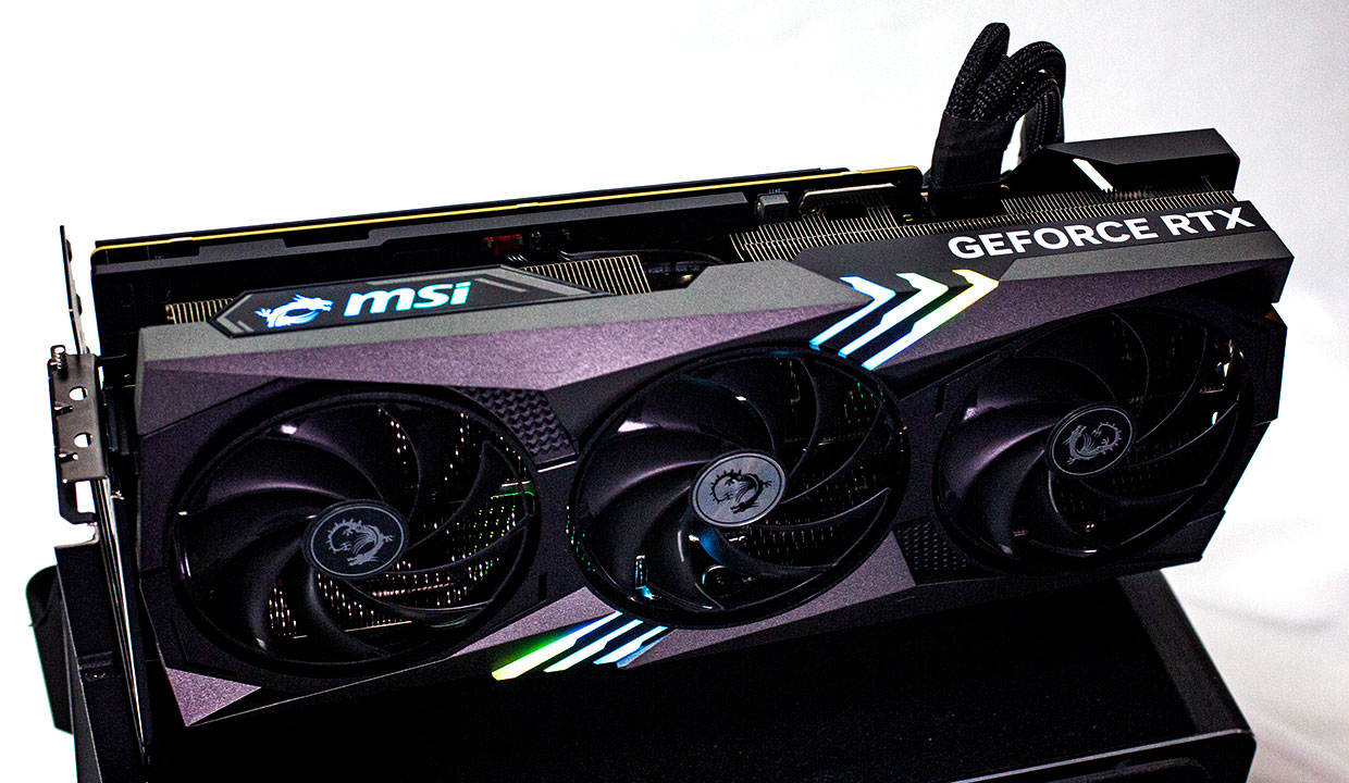
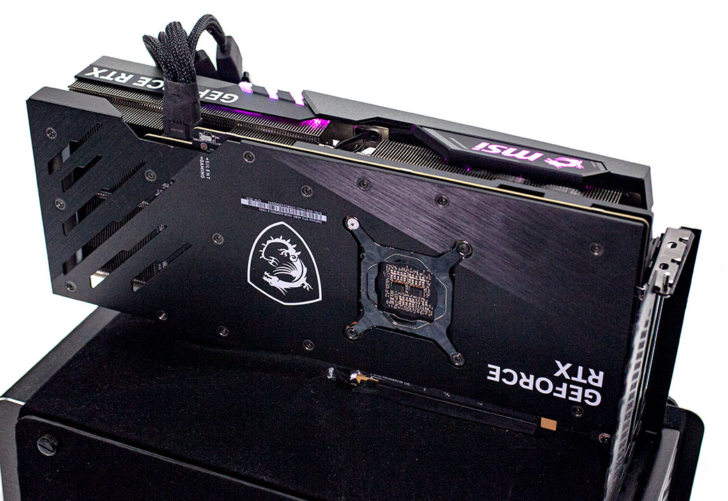
MSI has integrated two RGB illuminated elements in the front cooler.
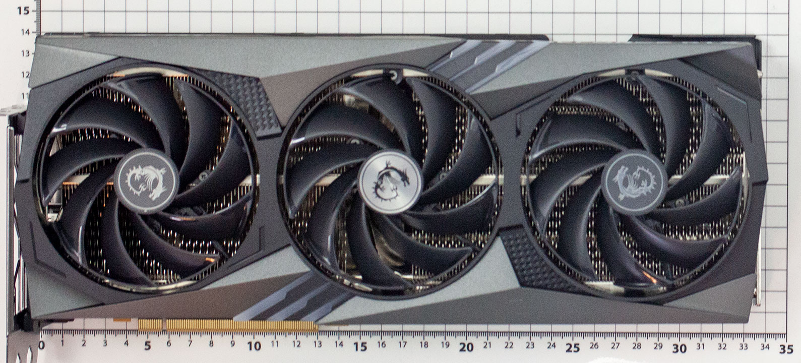
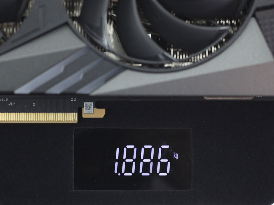
Dimensions of the card are 34.0 x 14.0 cm, and it weighs 1886 g.
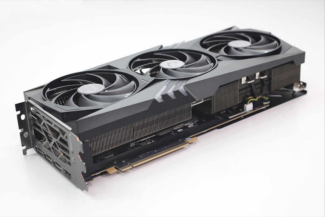
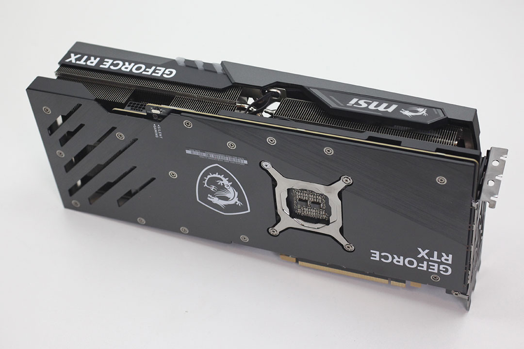
Installation requires three slots in your system.
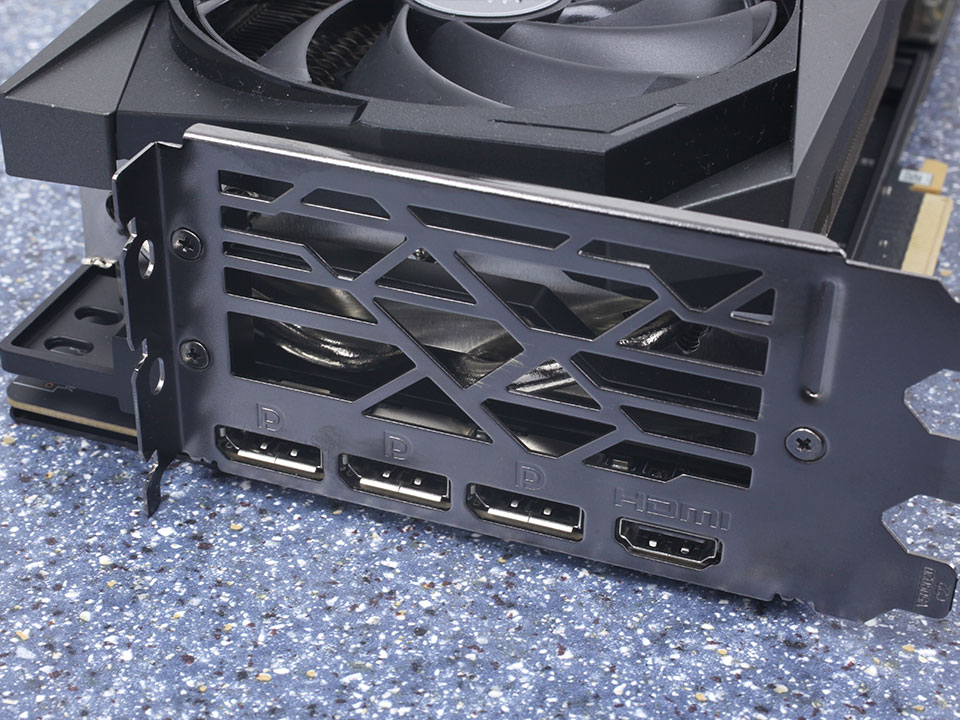
Display connectivity includes three standard DisplayPort 1.4a ports and one HDMI 2.1a (same technology as Ampere).
NVIDIA introduced the concept of dual NVDEC and NVENC Codecs with the Ada architecture. This means there are two independent sets of hardware-accelerators; so you can encode and decode two streams of video in parallel or one stream at double the FPS rate. The new 8th Gen NVENC now accelerates AV1 encoding, besides HEVC. You also get an "optical flow accelerator" unit that is able to calculate intermediate frames for videos, to smooth playback. The same hardware unit is used for frame generation in DLSS 3.
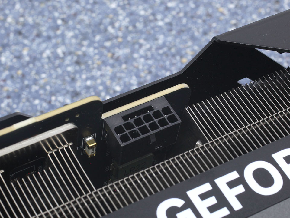
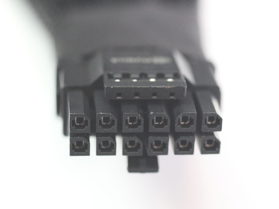

The card uses the new 12+4 pin ATX 12VHPWR connector, which is rated for up to 600 W of power draw. An adapter cable from 3x PCIe 8-pin is included (which is rated for up to 450 W). Of course the 4x 8-pin to 16-pin adapter cables from RTX 4090 will also work with the RTX 4080, but the card won't need that much power.
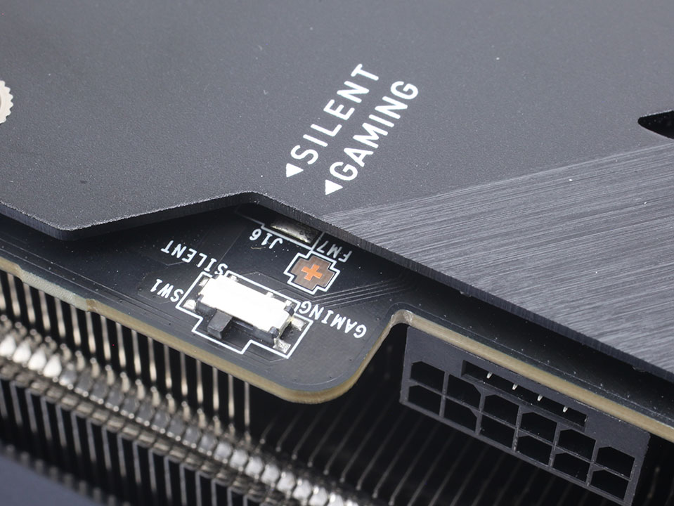
This BIOS switch lets you toggle from the default quiet BIOS to the gaming BIOS, which runs a more aggressive fan curve.
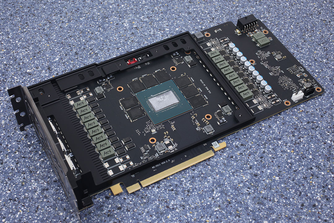
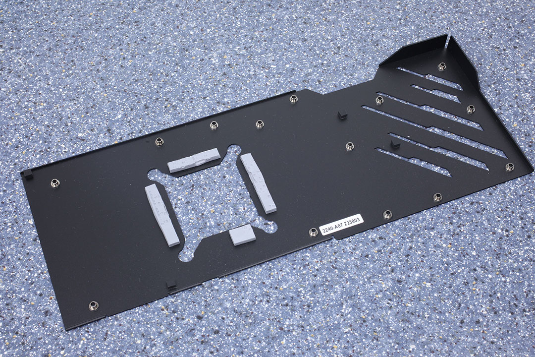
Teardown
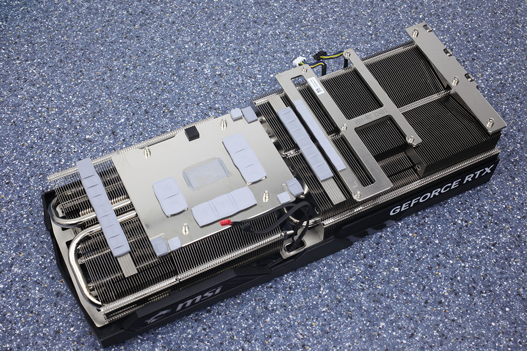
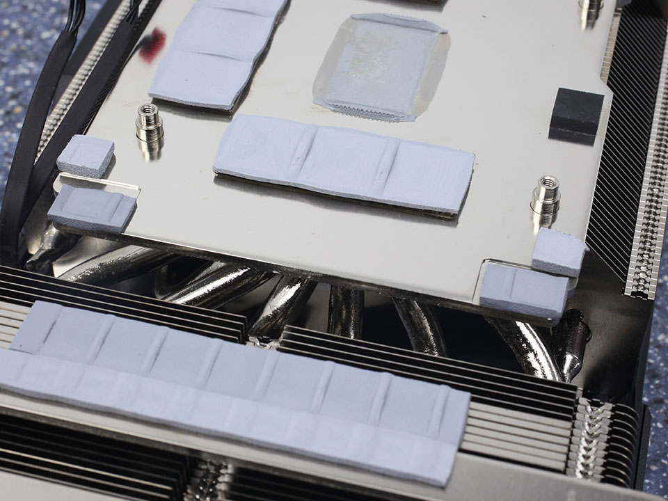
MSI'S thermal solution is big and powerful. While the Suprim X has a vapor-chamber, the Gaming X Trio has a classic baseplate, which soaks up heat from the GPU quickly and moves it through eight heatpipes to the heatsink. The main heatsink also provides cooling for the VRM and memory chips.
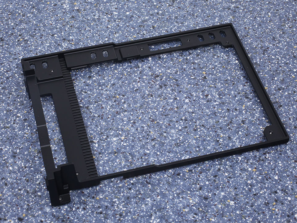

Once the main cooler assembly is removed, a metal frame becomes visible, which helps protect against bending and sagging.
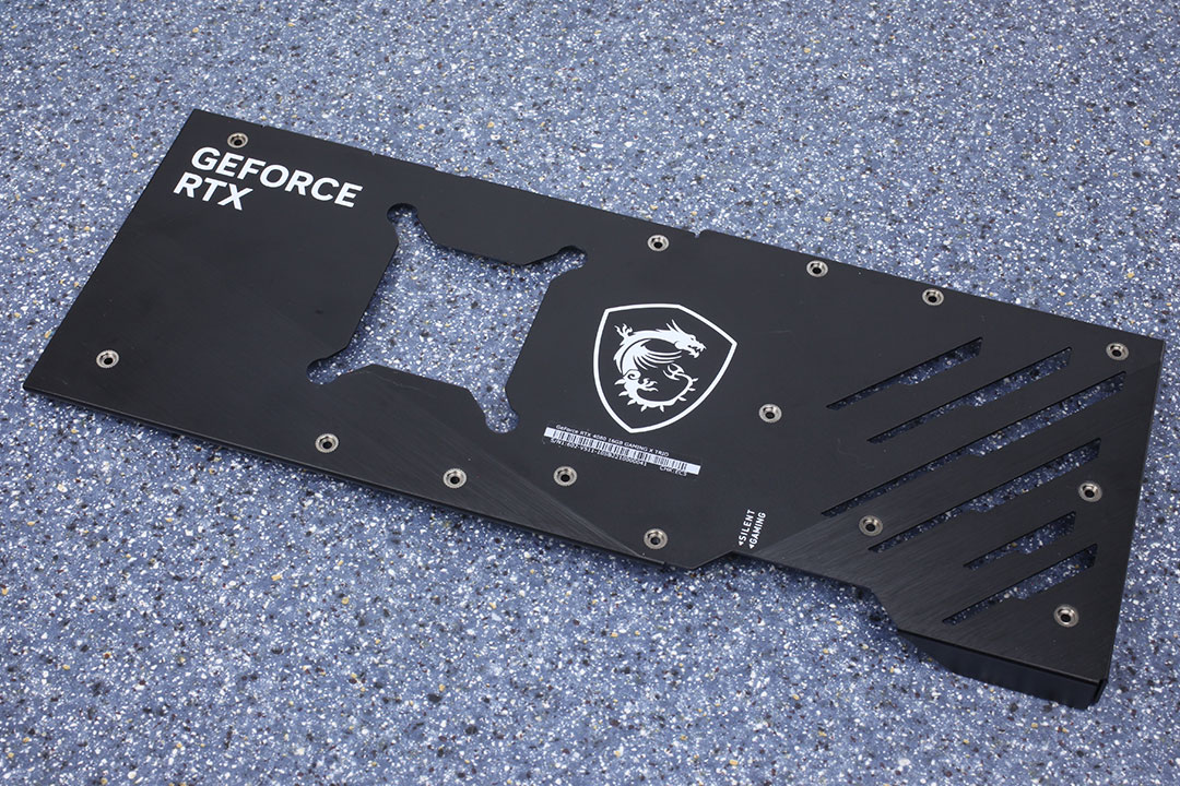
The backplate is made of metal and protects the card against damage during installation and handling.
High-resolution PCB Pictures
These pictures are for the convenience of volt modders and people who would like to see all the finer details on the PCB. Feel free to link back to us and use these in your articles, videos or forum posts.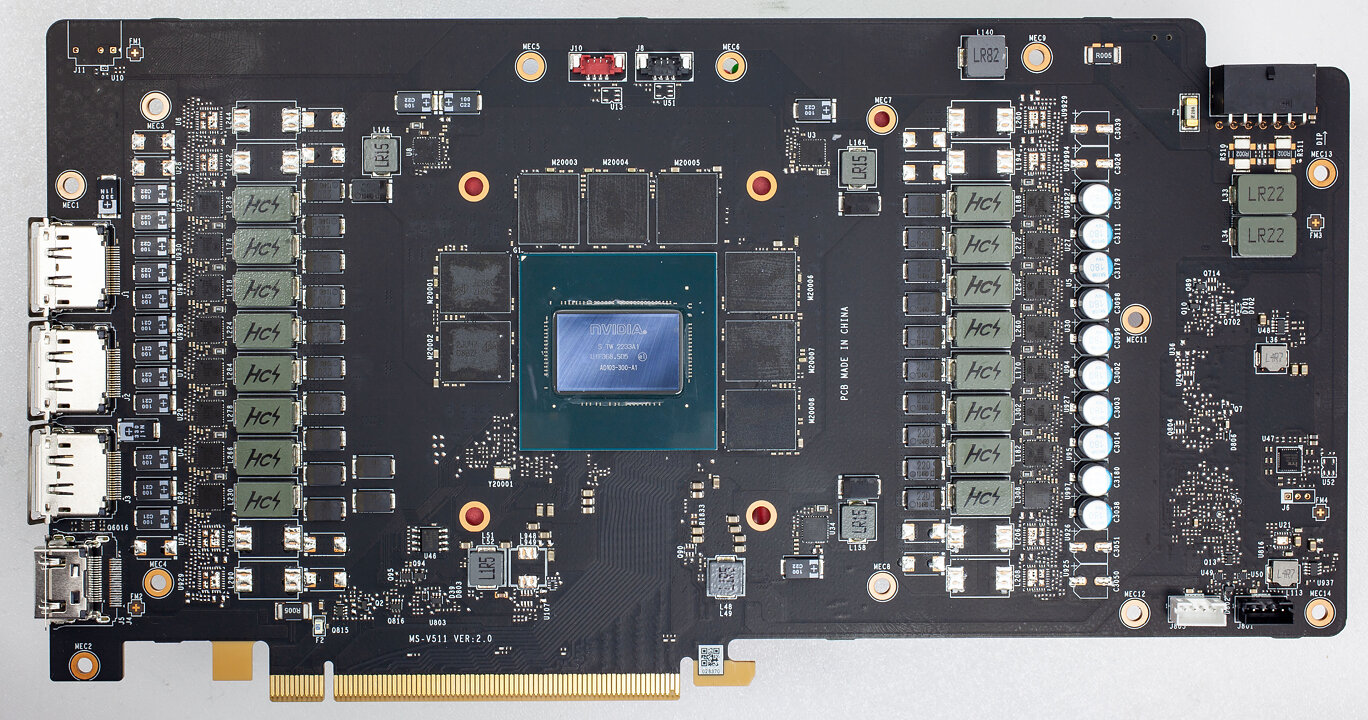
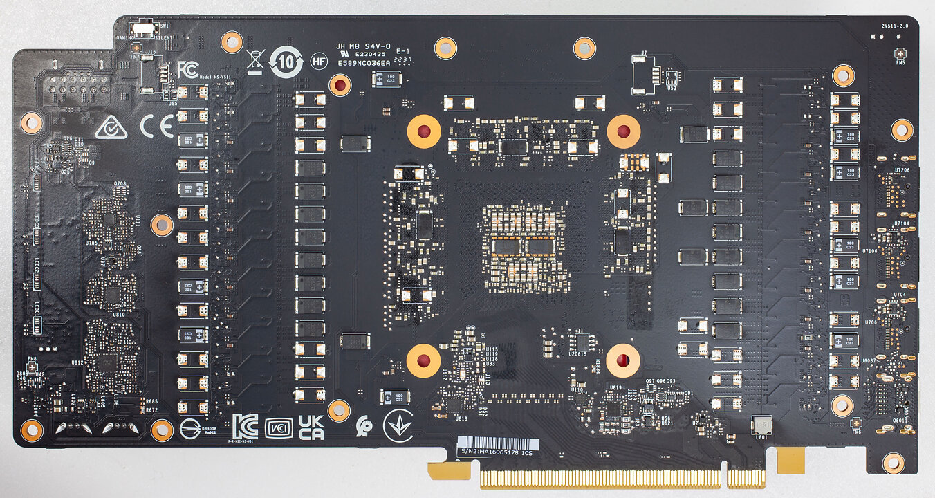
High-resolution versions are also available (front, back).
Circuit Board (PCB) Analysis
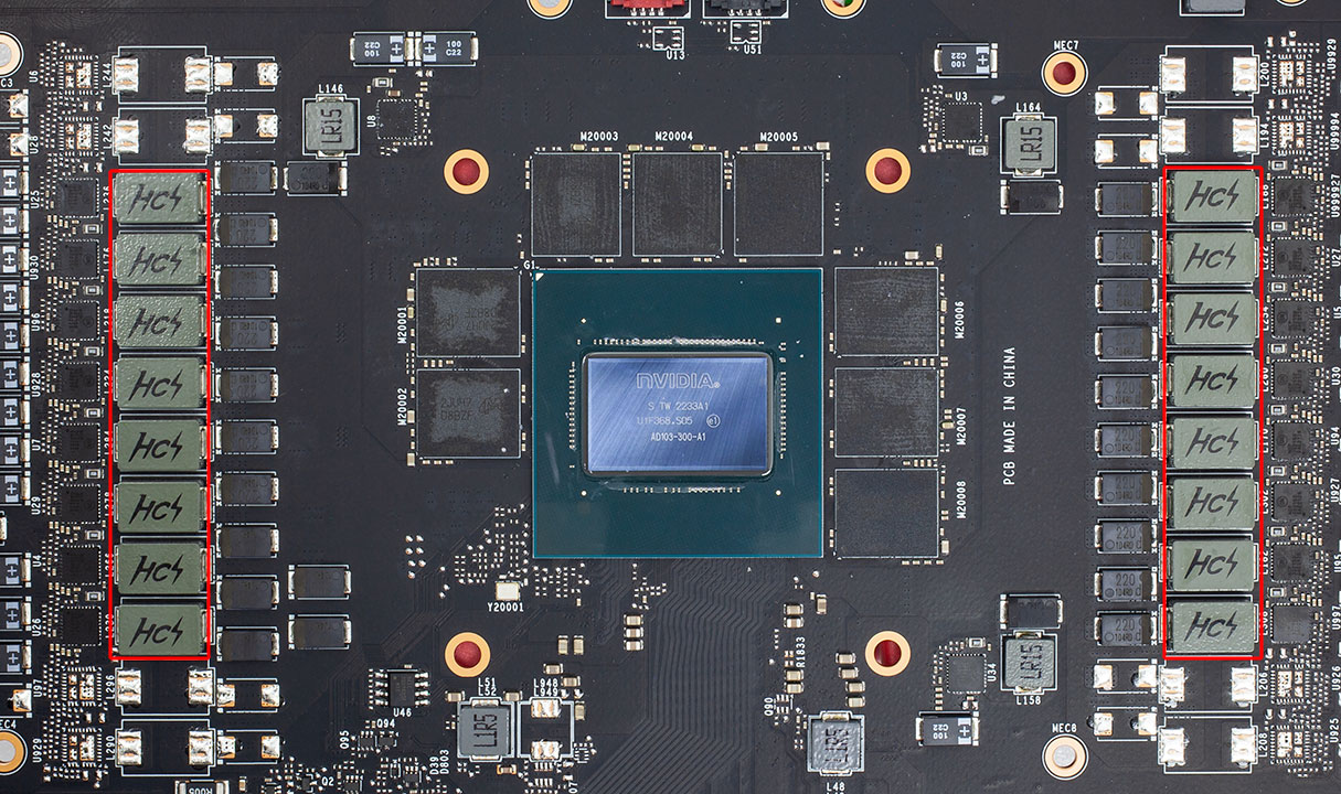

GPU voltage is a 16-phase design, managed by a UPI uP9512R controller.

OnSemi NCP302150 DrMOS components are used for GPU voltage; they are rated for 50 A of current each.


Memory voltage is a three-phase design, managed by a uPI uP9529Q controller.

For memory, OnSemi NCP3102150 DrMOS with a 50 A rating are used, too.

The GDDR6X memory chips are made by Micron and carry the model number D8BZF, which decodes to MT61K512M32KPA-24. They are specified to run at 1500 MHz (24 Gbps effective).
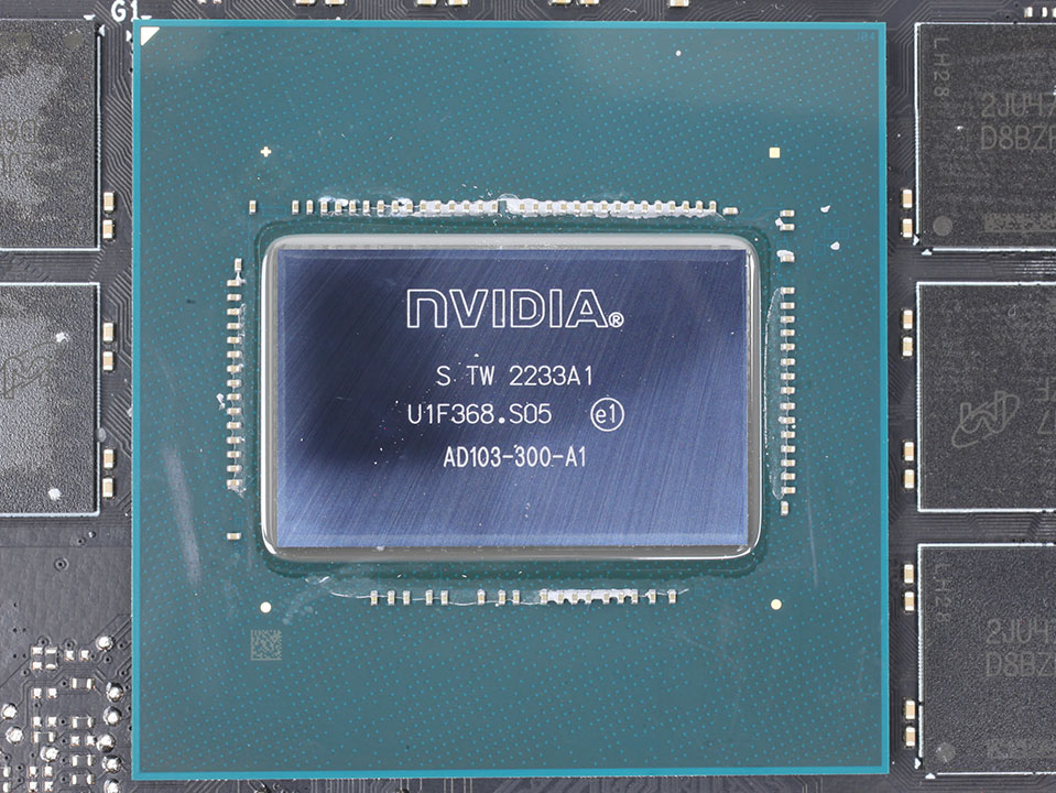
NVIDIA's AD103 graphics processor is the company's second Ada Lovelace GPU. It is built using a 5 nanometer process at TSMC Taiwan, with a transistor count of 45.9 billion and a die size of 379 mm².
Our Patreon Silver Supporters can read articles in single-page format.
May 9th, 2024 13:25 EDT
change timezone
Latest GPU Drivers
New Forum Posts
- TPU's Nostalgic Hardware Club (18504)
- Battery swap for cyberpower UPS (66)
- Last game you purchased? (275)
- Current Sales, Bundles, Giveaways (10231)
- What's a good option for a digital touchless thermometer? (17)
- Epic Games launcher's ridiculous CPU usage (33)
- Only some humans can see refresh rates faster than others, I am one of those humans. (233)
- Your way of cooling your PC? (86)
- AM5 boot times improve RADICALLY with memory context restore enabled (1)
- Microsoft butchering Xbox Studios (26)
Popular Reviews
- CHERRY XTRFY M64 Pro Review
- Corsair iCUE Link RX120 RGB 120 mm Fan Review
- Bykski CPU-XPR-C-I CPU Water Block Review - Amazing Value!
- Finalmouse UltralightX Review
- Upcoming Hardware Launches 2023 (Updated Feb 2024)
- AMD Ryzen 7 7800X3D Review - The Best Gaming CPU
- Corsair MP700 Pro SE 4 TB Review
- Cougar Hotrod Royal Gaming Chair Review
- ASUS Radeon RX 7900 GRE TUF OC Review
- Meze Audio LIRIC 2nd Generation Closed-Back Headphones Review
Controversial News Posts
- Intel Statement on Stability Issues: "Motherboard Makers to Blame" (262)
- AMD to Redesign Ray Tracing Hardware on RDNA 4 (206)
- Windows 11 Now Officially Adware as Microsoft Embeds Ads in the Start Menu (167)
- NVIDIA to Only Launch the Flagship GeForce RTX 5090 in 2024, Rest of the Series in 2025 (144)
- Sony PlayStation 5 Pro Specifications Confirmed, Console Arrives Before Holidays (119)
- AMD's RDNA 4 GPUs Could Stick with 18 Gbps GDDR6 Memory (114)
- NVIDIA Points Intel Raptor Lake CPU Users to Get Help from Intel Amid System Instability Issues (106)
- AMD Ryzen 9 7900X3D Now at a Mouth-watering $329 (104)