 45
45
MSI GeForce RTX 4090 Gaming X Trio Review
Test Setup »High-resolution PCB Pictures
These pictures are for the convenience of volt modders and people who would like to see all the finer details on the PCB. Feel free to link back to us and use these in your articles, videos or forum posts.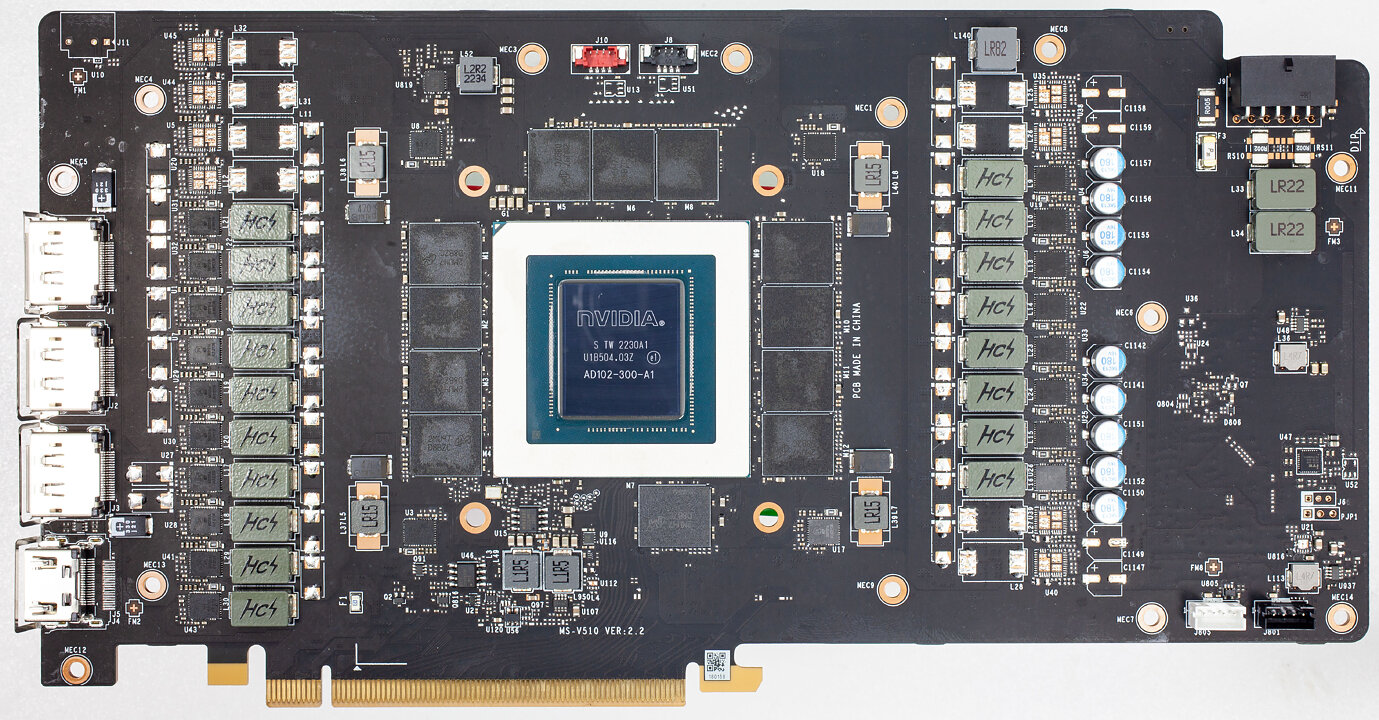
High-resolution versions are also available (front, back).
Circuit Board (PCB) Analysis


GPU voltage is a massive 18-phase design managed by a Monolithic Power Systems MP2891 controller, which also handles memory voltage.
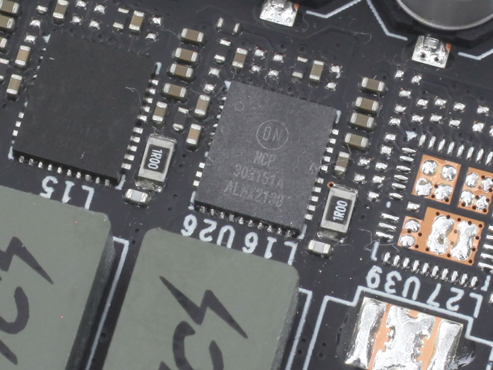
OnSemi NCP303151A DrMOS components are used for GPU voltage; they are rated for 50 A of current each.

Memory voltage is a four-phase design, managed by the same MP2891 that's uses for GPU voltage.

For memory, OnSemi NCP303151A DrMOS with a 50 A rating are used too.

The GDDR6X memory chips are made by Micron and carry the model number D8BZC, which decodes to MT61K512M32KPA-21:U. They are specified to run at 1313 MHz (21 Gbps effective).

NVIDIA's AD102 graphics processor is the company's flagship Ada Lovelace GPU. It's the world's first 5 nanometer GPU, built at TSMC Taiwan with a transistor count of 76.3 billion and a die size of 608 mm².
May 3rd, 2024 09:52 EDT
change timezone
Latest GPU Drivers
New Forum Posts
- Which PSU to take? (45)
- Ryzen Owners Zen Garden (7292)
- Your PC ATM (34542)
- What's your latest tech purchase? (20418)
- ASRock Deskmini Owner's Club (29)
- Is this Sapphire PULSE RX 5600 XT legit or fake? (31)
- Just for lolz, Post your 3DMark2001SE Benchmark scores! (85)
- Does not show part of the data RTX 4070 VENTUS 3X E 12G OC (3)
- Arctic MX-6 shelf life is just a couple months? (81)
- Old high quality PSU, or semi-old mid-quality PSU? (50)
Popular Reviews
- HYTE THICC Q60 240 mm AIO Review
- ASRock NUC BOX-155H (Intel Core Ultra 7 155H) Review
- Meze Audio LIRIC 2nd Generation Closed-Back Headphones Review
- Montech Sky Two GX Review
- Ugreen NASync DXP4800 Plus Review
- Upcoming Hardware Launches 2023 (Updated Feb 2024)
- Team Group T-Force Vulcan ECO DDR5-6000 32 GB CL38 Review
- MOONDROP x Crinacle DUSK In-Ear Monitors Review - The Last 5%
- AMD Ryzen 7 7800X3D Review - The Best Gaming CPU
- Logitech G Pro X Superlight 2 Review - Updated with 4000 Hz Tested
Controversial News Posts
- Intel Statement on Stability Issues: "Motherboard Makers to Blame" (232)
- Windows 11 Now Officially Adware as Microsoft Embeds Ads in the Start Menu (167)
- Sony PlayStation 5 Pro Specifications Confirmed, Console Arrives Before Holidays (117)
- AMD's RDNA 4 GPUs Could Stick with 18 Gbps GDDR6 Memory (114)
- NVIDIA Points Intel Raptor Lake CPU Users to Get Help from Intel Amid System Instability Issues (106)
- AMD "Strix Halo" Zen 5 Mobile Processor Pictured: Chiplet-based, Uses 256-bit LPDDR5X (103)
- AMD Ryzen 9 7900X3D Now at a Mouth-watering $329 (103)
- TechPowerUp Hiring: Reviewers Wanted for Motherboards, Laptops, Gaming Handhelds and Prebuilt Desktops (93)