 19
MSI MPG Ai1600TS Review
Test Methodology »Internals
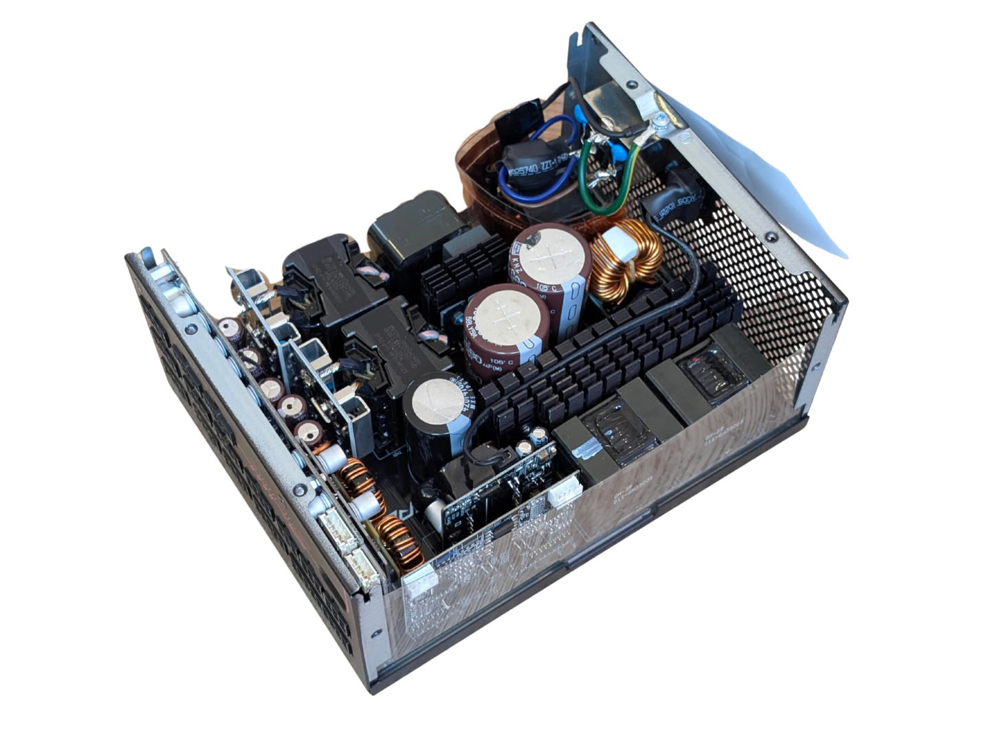
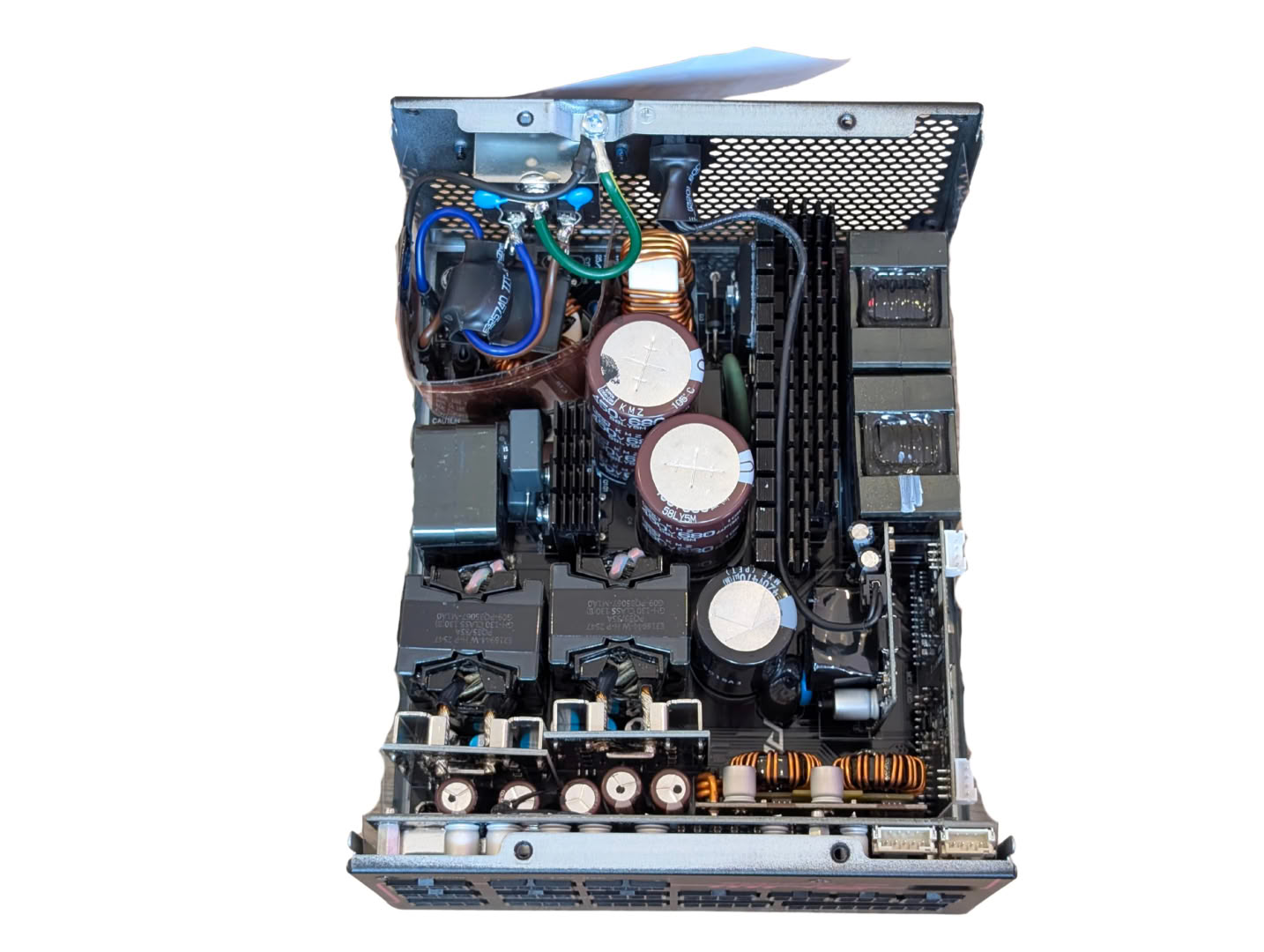
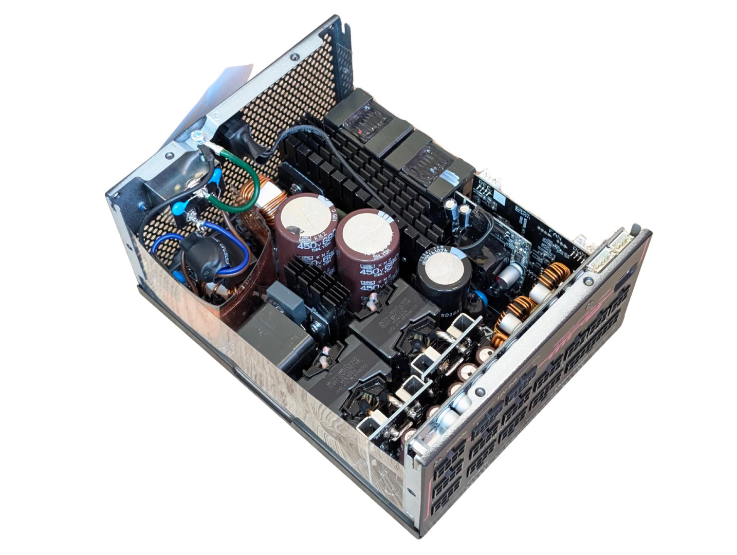
First impressions on opening the case are impressive. The components are packed well but not overcrowded, build quality feels solid and nothing moves that shouldn't.
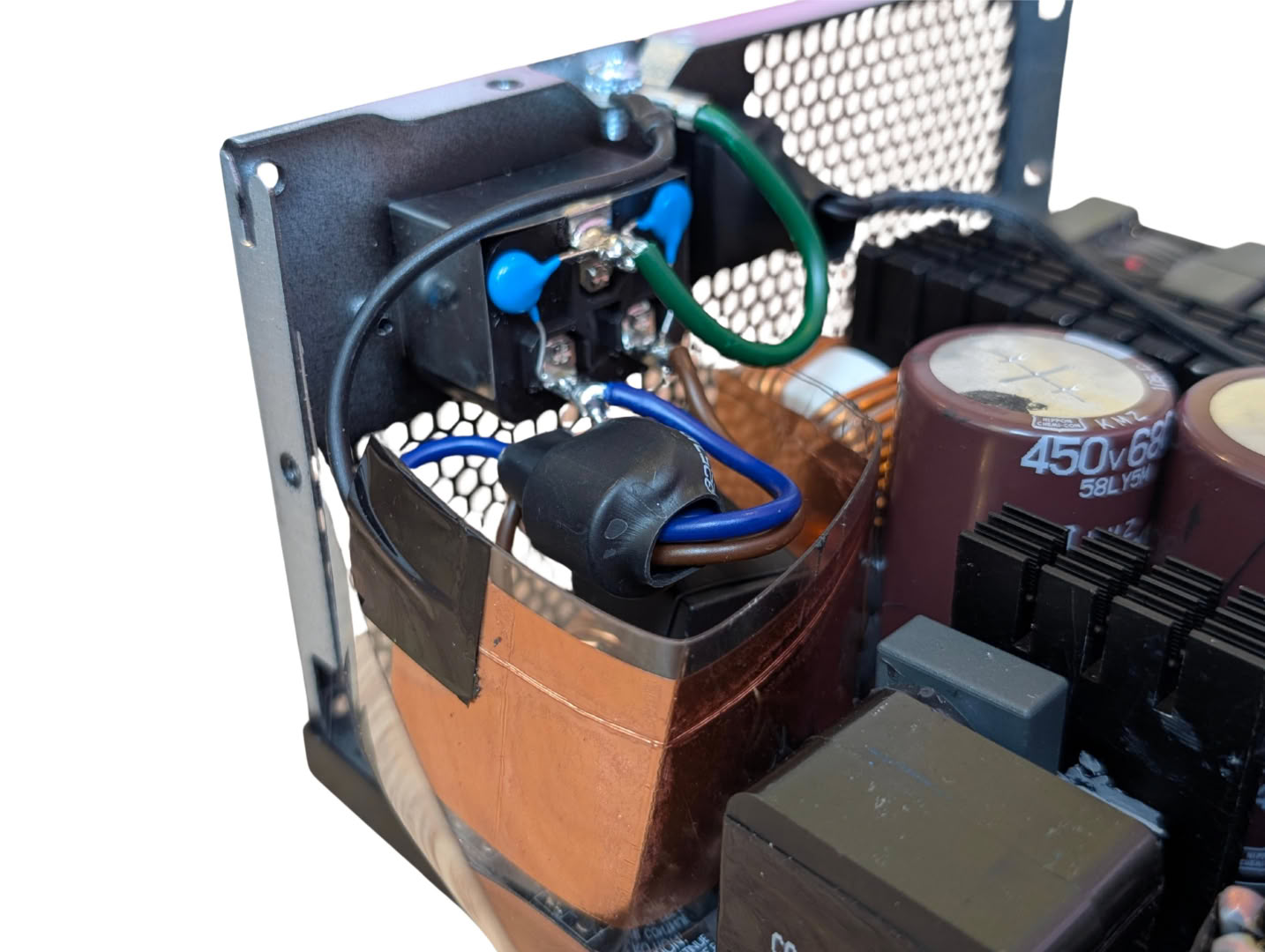
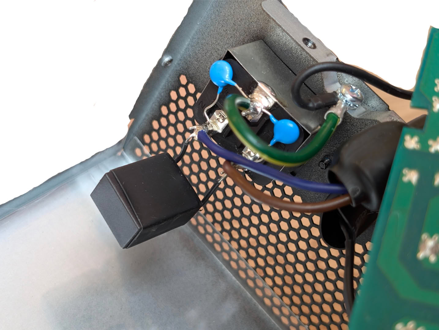
Filtering at the mains terminal is excellent. We have a pair of Y caps and an X cap on the back of the connector itself, a choke along the cables to the main board, and a grounded copper plate shielding the mains input components from switching noise.
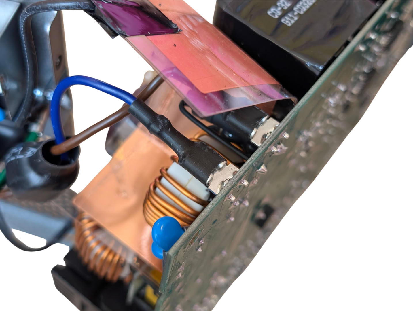
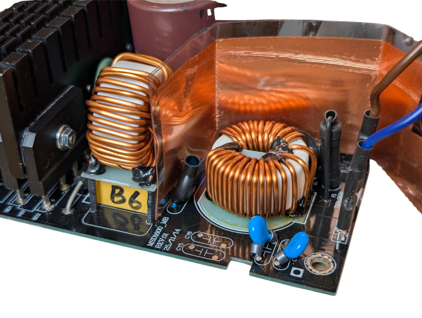
Mains power comes in to the main board via spade terminals and then through fuse F1. There are a pair of large chokes here, a pair of Y caps with ferrite beads around their legs, and a pair of X caps hiding under the second choke. In total for input filtering, there are:
2× X-capacitors
5× Y-capacitors
2× Common-mode chokes
1× MOV (Metal Oxide Varistor)
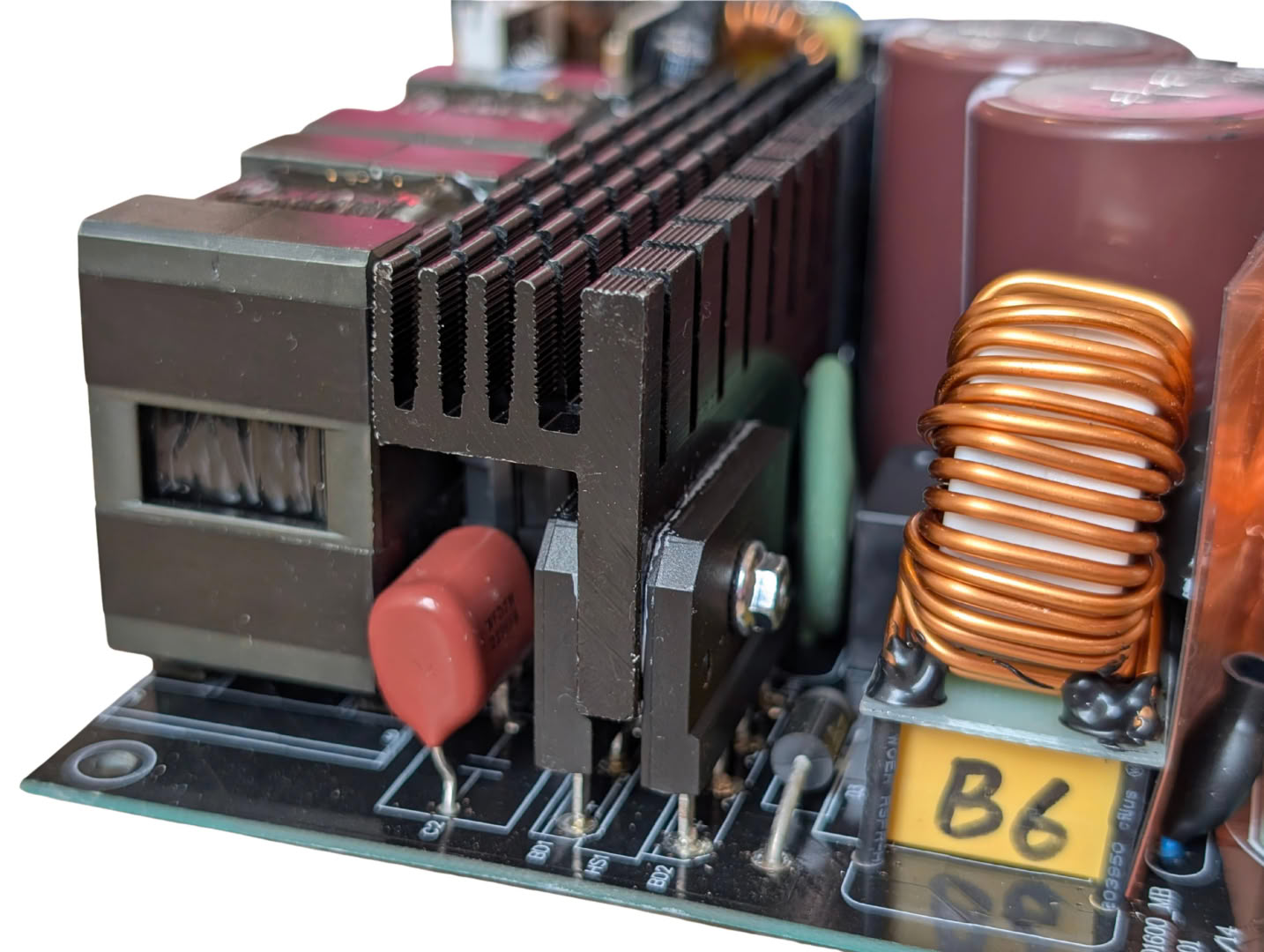
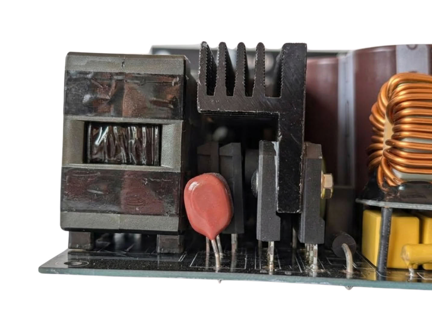
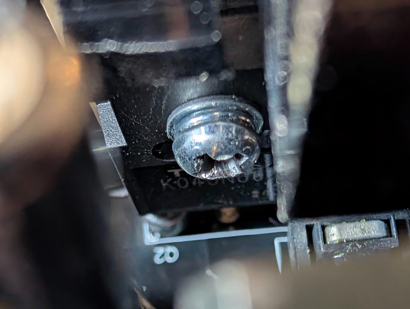
There are a pair of large full bridge rectifiers clamped to a heatsink, also shared by some MOSFETs handling PFC. The unit is built on a semi-digital, interleaved bridgeless PFC layout that works in tandem with a full-bridge LLC resonant converter.
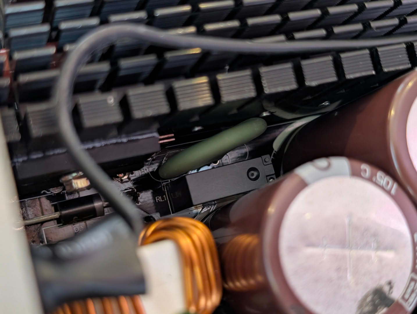
Inrush suppression is handled after rectification, bypassed by this relay once the caps are sufficiently charged.
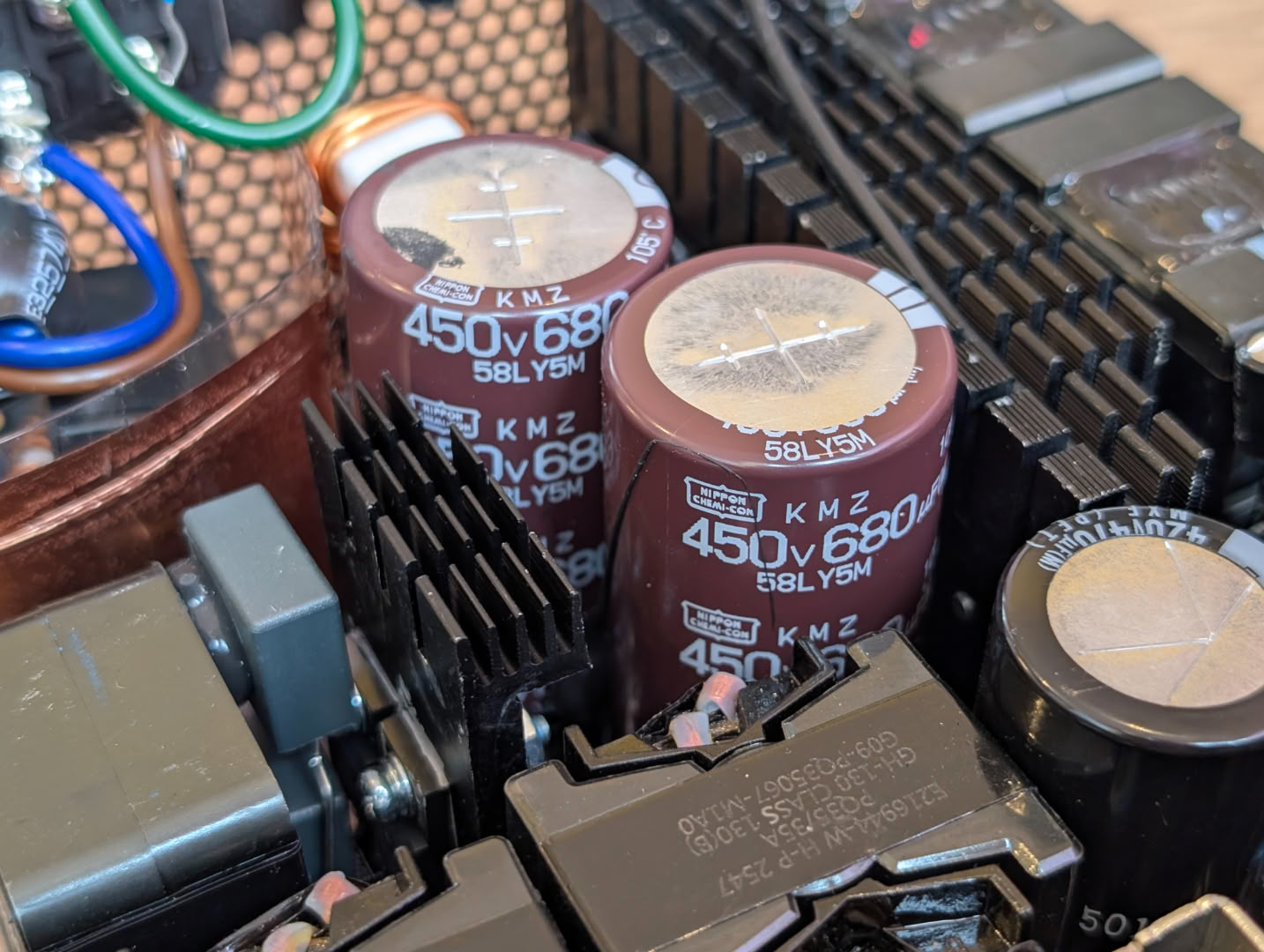
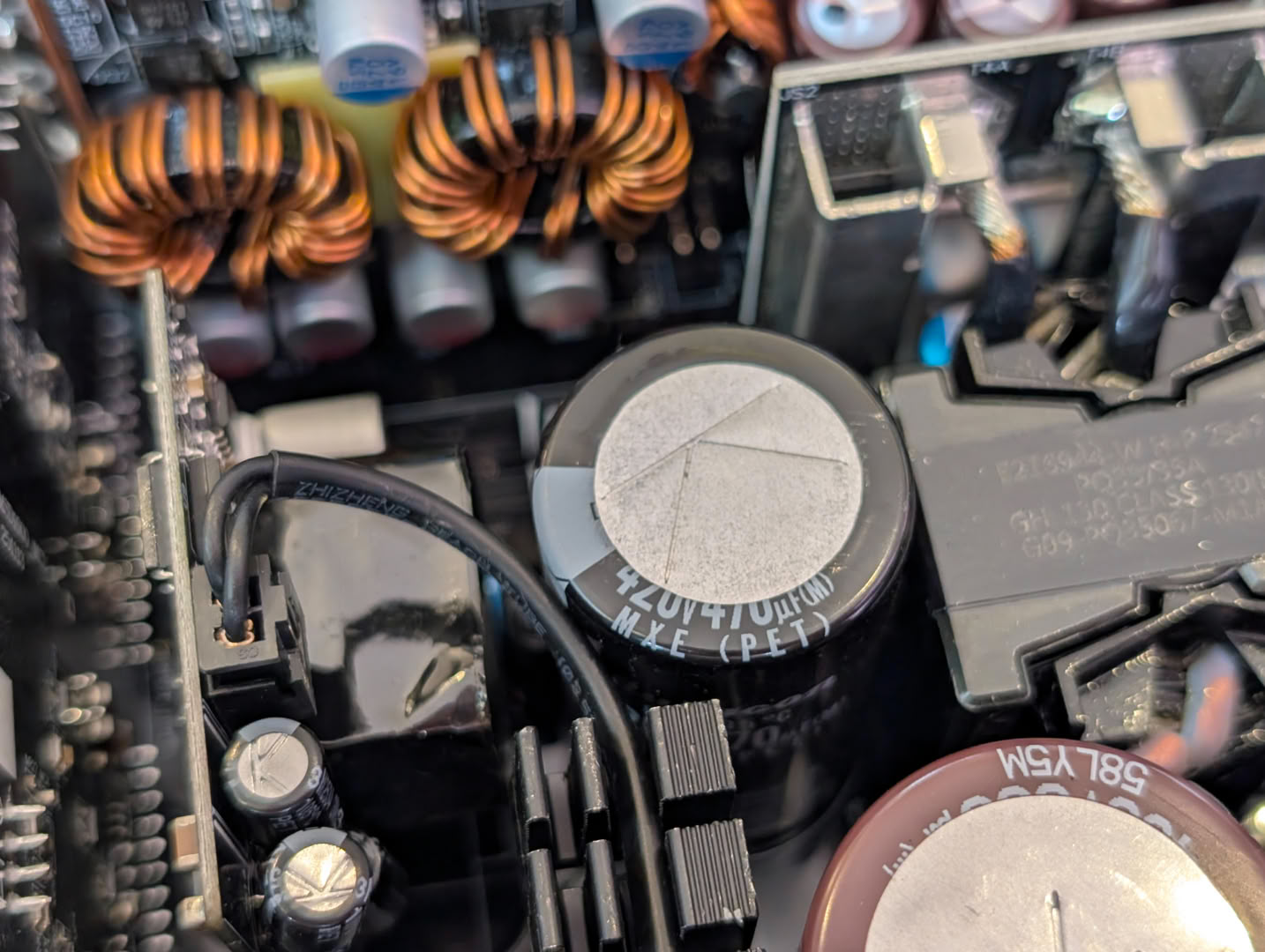
For bulk caps, we have premium 105°C-rated Japanese hardware for the primary stage. The configuration pairs Nippon Chemi-Con units (KMZ series, 450 V, 680 µF) with a Rubycon capacitor (420 V, 470 µF) to achieve a total capacitance of 1830 µF.
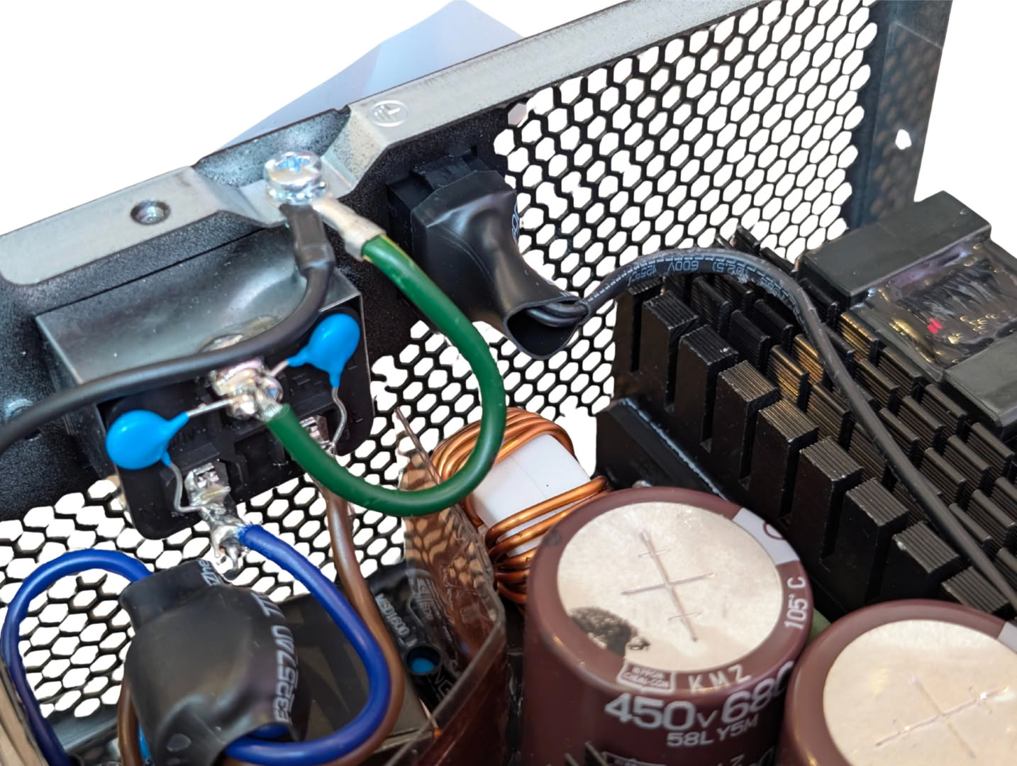
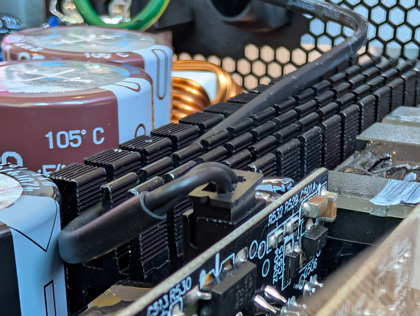
This is the first unit I have seen where the power switch on the back does not directly break mains power from entering the supply. The switch here instead activates a standby circuit and disables/enables the main DC-DC converters which would come on when the Power signal on the motherboard connector is grounded. This means even with the switch in the off position, current is still flowing into the power supply and bulk voltage is still being held.
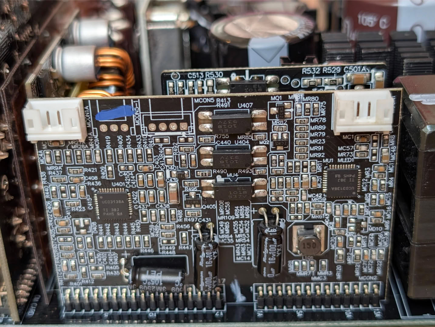
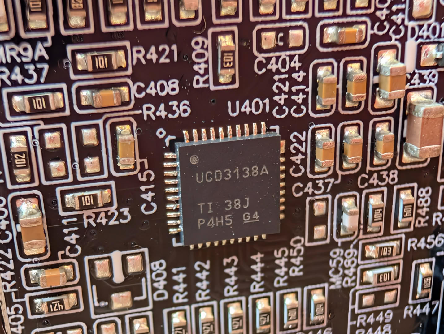
A pair of MCUs handle all the complex functionality and control of this innovative power supply.
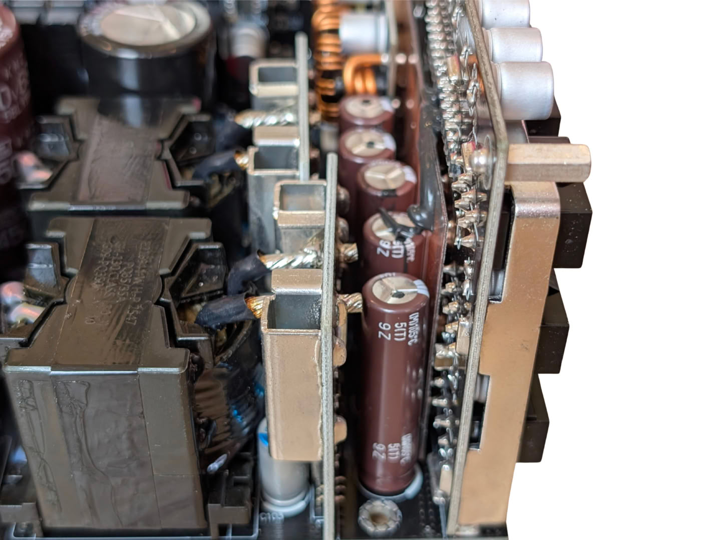
Moving to the secondary side, it relies on a combination of synchronous rectification and DC-to-DC converters. Unlike other power supplies we have covered, the MOSFETs are mounted to thick daughterboards with metal bars as thermal mass.
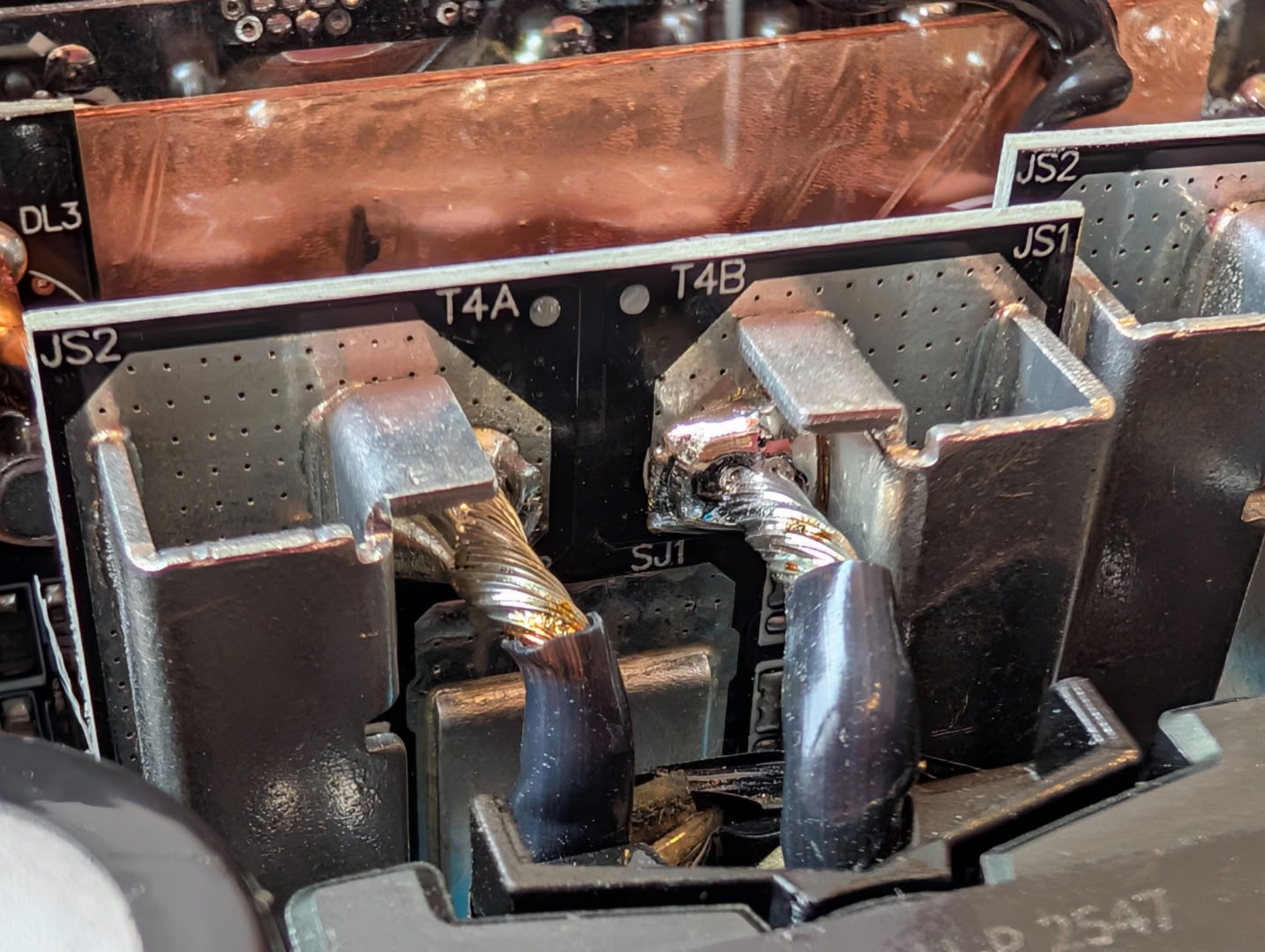
The transformers are soldered directly to the output boards.
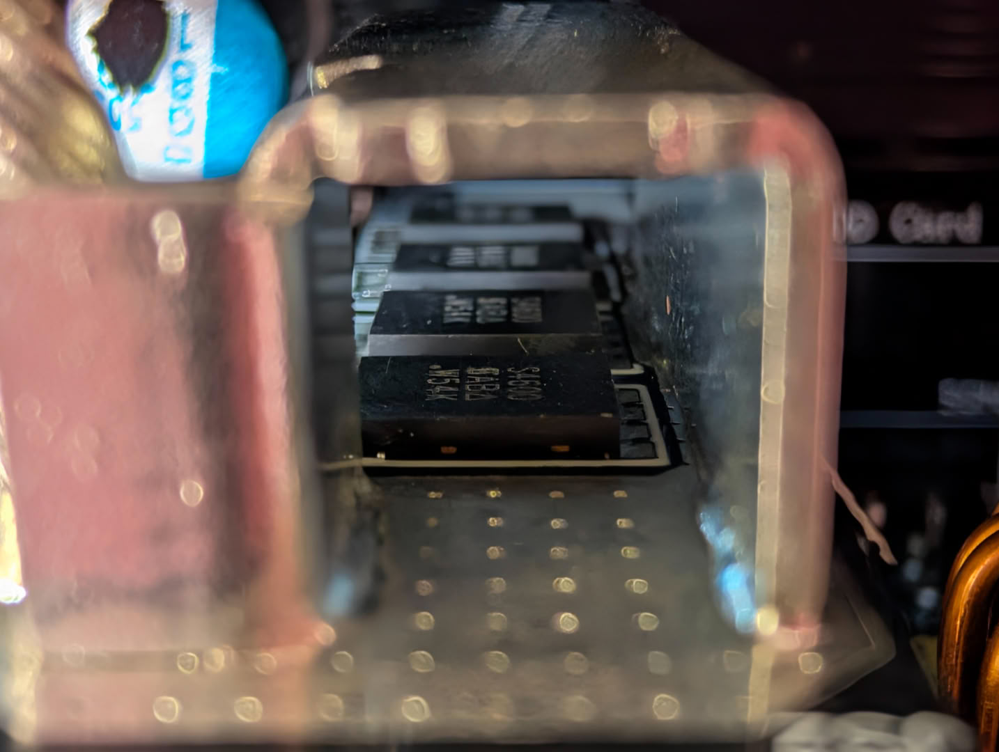
The MOSFETs are surface mount SiRS4600DP by Vishay, 60 V TrenchFET with a staggering 359 A silicon limit and 1.15 mΩ RDS.
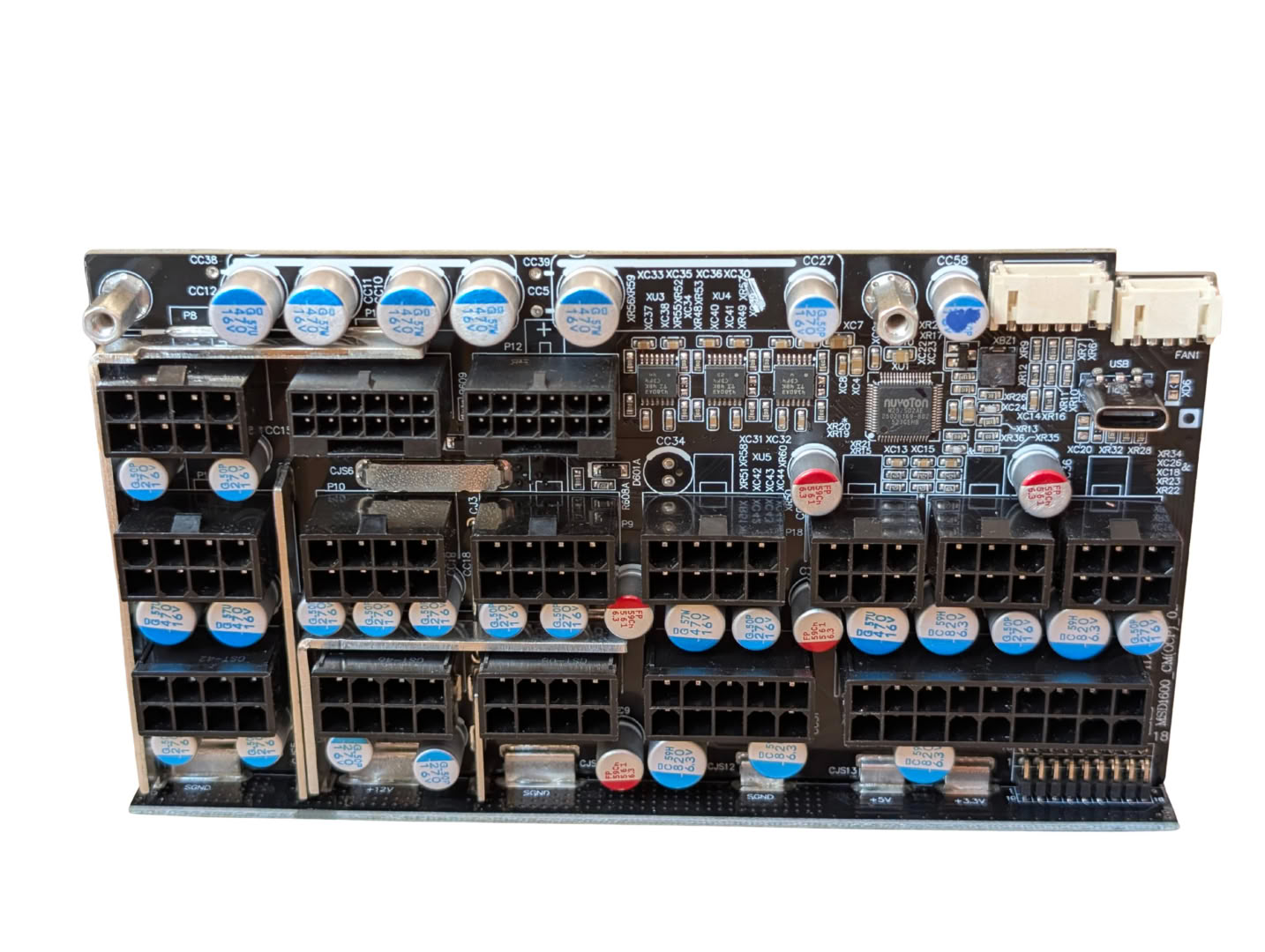
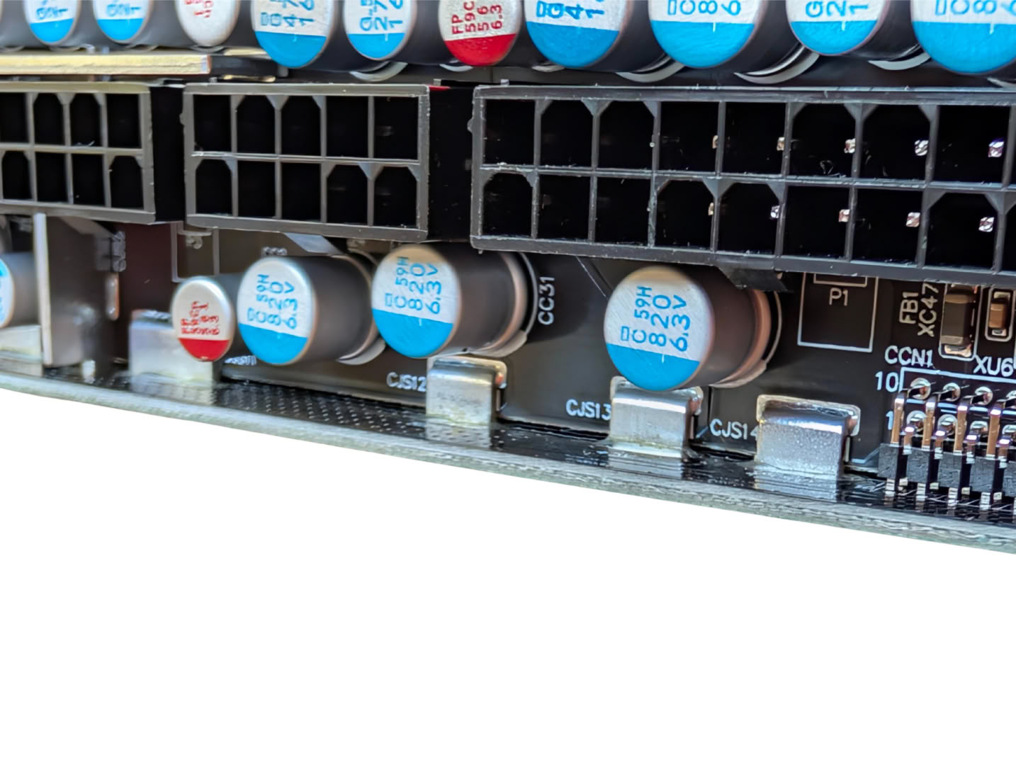
The output connector board is soldered to the main board with heavy-duty lugs. These are much better than using multiple pins or soldered cables. There are capacitors alongside each of the connectors to ensure the voltage at each is stable and clean.
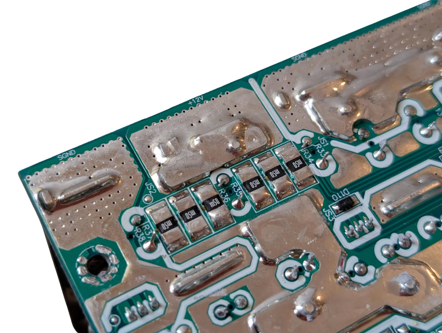
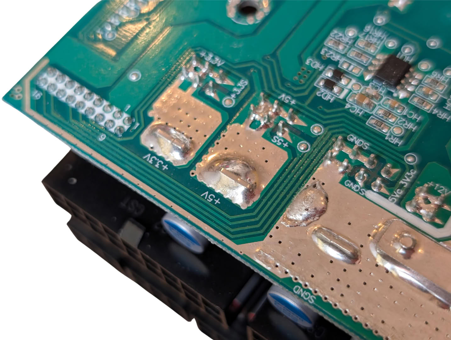
The soldering quality is superb, and the finish is very neat.
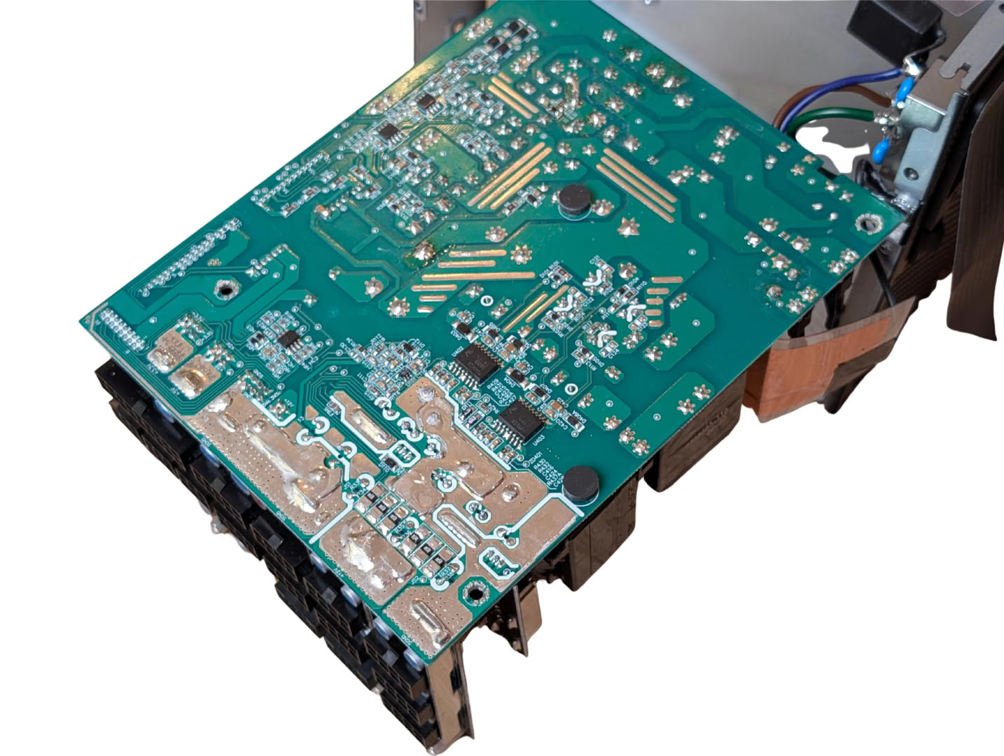
The back side of the PCB houses a few components, which is to be expected with such a complex unit. The layout and finish again overall is very tidy.
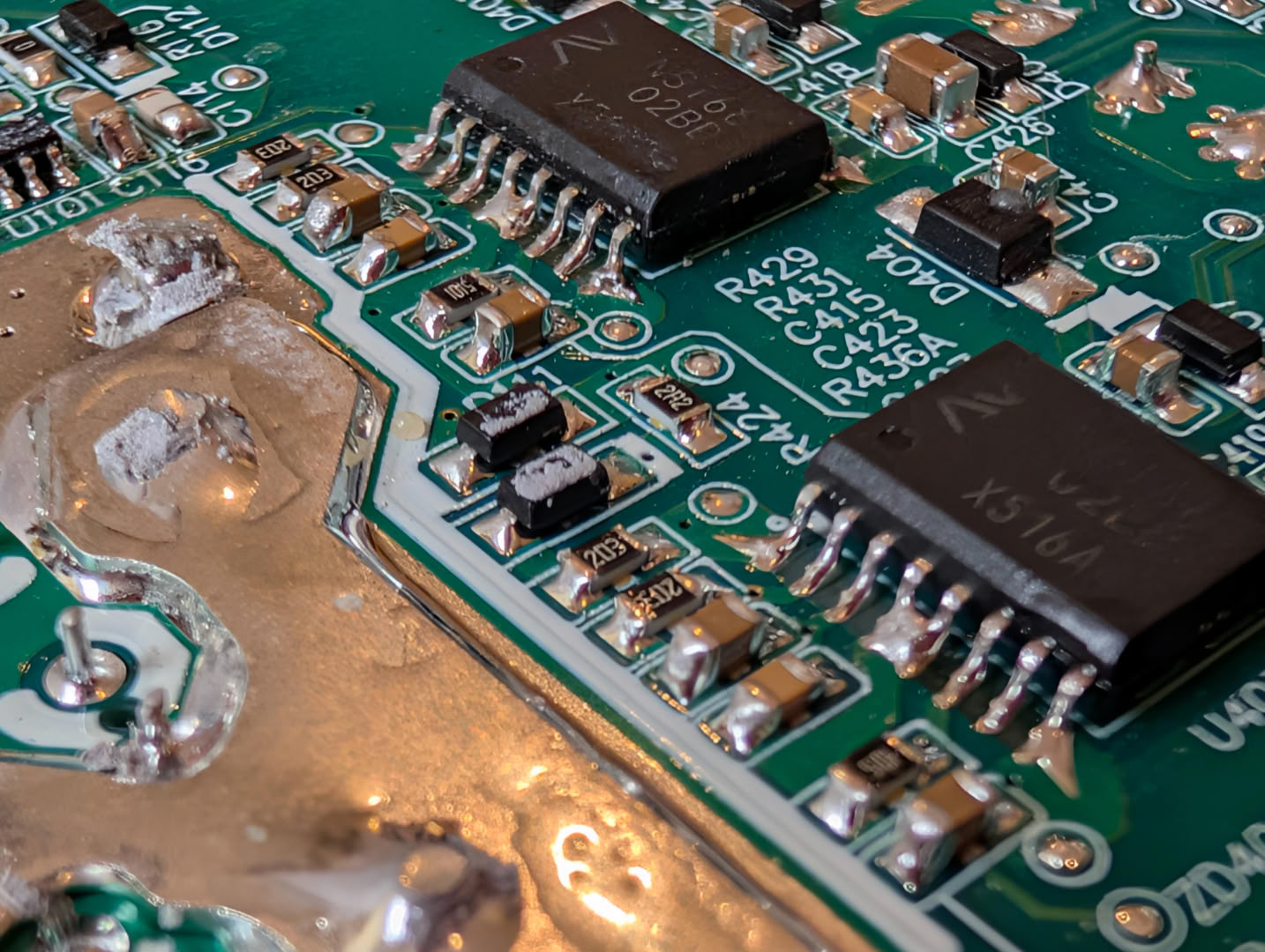
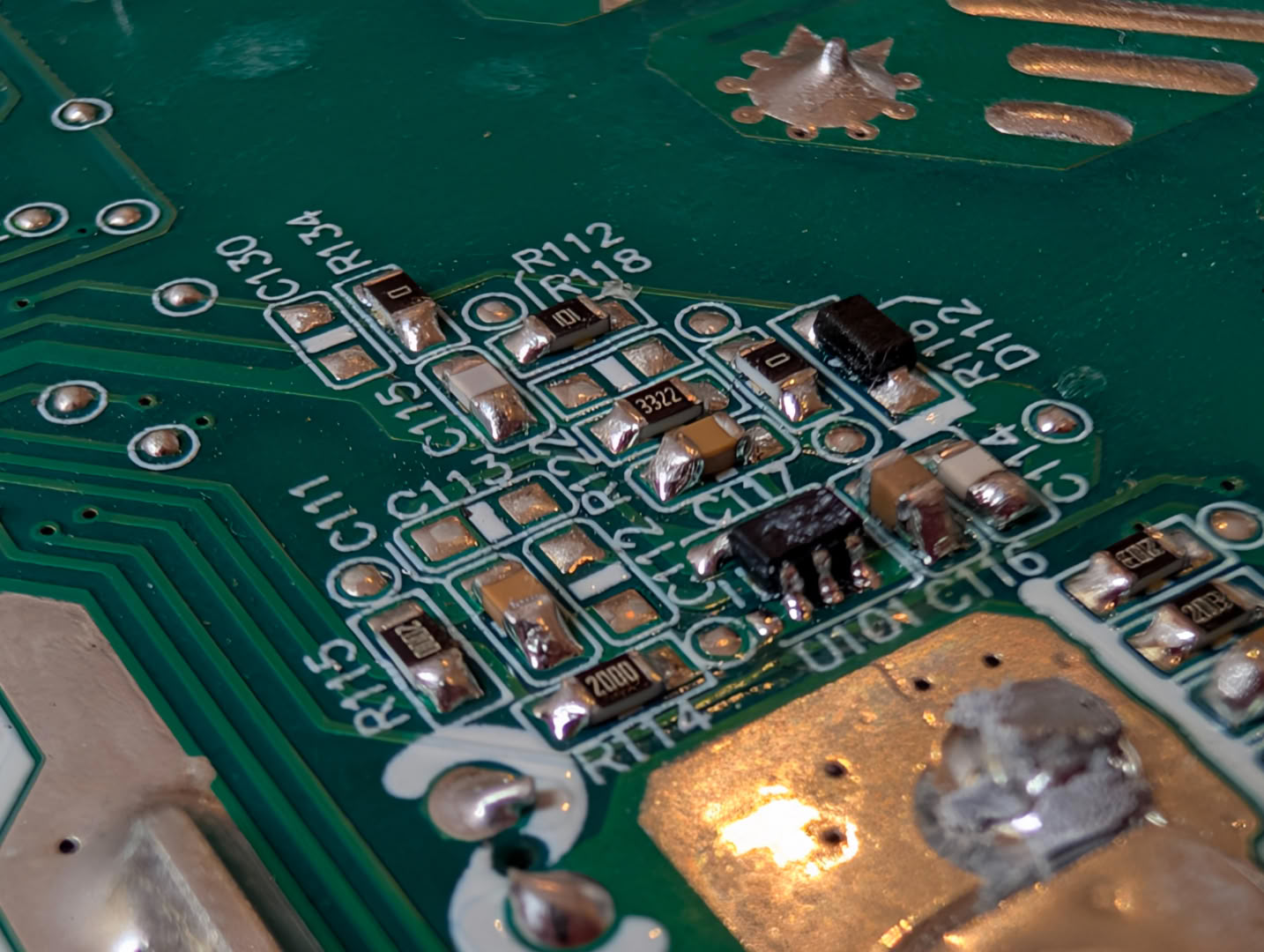
The soldering quality of SMD components throughout is fine, a little uneven in places but definitely sufficient and the solder has flowed and set very well.
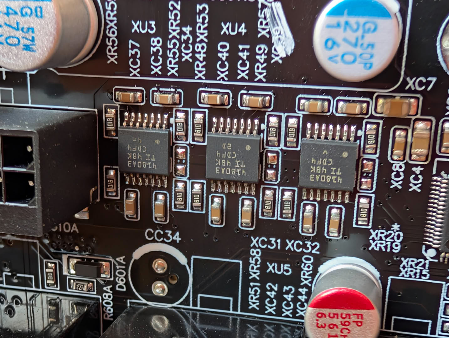
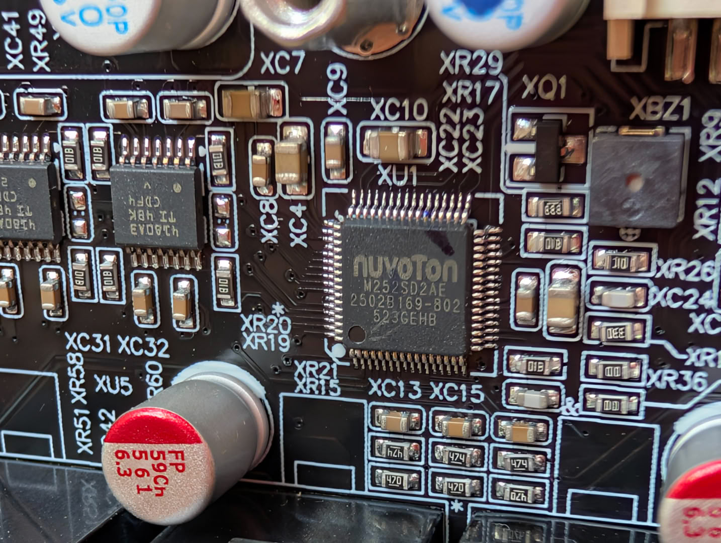
Taking a closer look at the output board reveals evidence of their innovative features. There are 3 INA4180 low/high side current-sense amplifiers, and an MCU, which will be for detecting and reporting currents across the 12V-2x6 connectors. The USB-C connector is also found alongside.
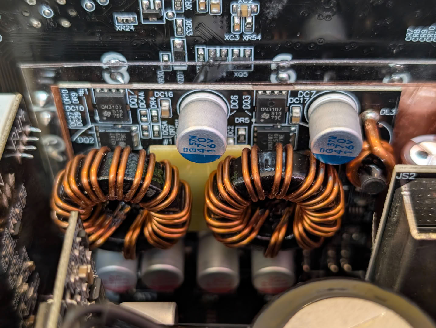
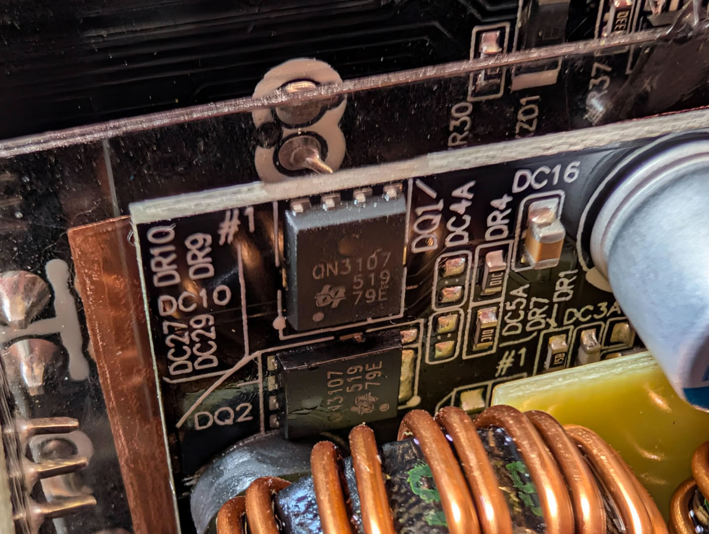
The lower voltage rails are created by DC-DC converters on this daughter board, using QN3107M6N MOSFETs.
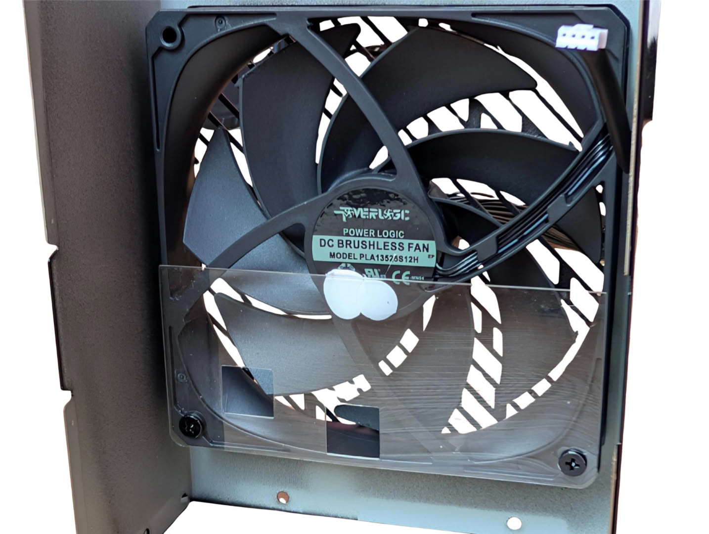
The fan selected here is a Powerlogic 135 mm PLA13525S12H, rated at 12 V 0.56 A with up to 2300 RPM.
Nov 18th, 2026 13:24 PST
change timezone
Latest GPU Drivers
New Forum Posts
- Can i play GTA 6 now? (Joke) (5)
- Very unusual two gaming-pc scenarios. (11)
- Dell Workstation Owners Club (3513)
- Any other old-timers here planning to play WoW Forever? (151)
- Time to upgrade CPU and MOBO (33)
- The Filthy, Rotten, Nasty, Helpdesk-Nightmare picture clubhouse (2876)
- WarpCoreBench scores! (67)
- Honestly, do you care about GTA VI? (144)
- Acer Predator BiFrost Radeon RX 9070 OC (9)
- DTS DCH Driver for Realtek HDA [DTS:X APO4 + DTS Interactive] (2814)
Popular Reviews
- Acemagic Retro X3 Review
- Upcoming Hardware Launches 2027 (Updated Nov 2026)
- AMD Zen 6 Technical Deep Dive
- ASUS ROG Strix B850-I Gaming Wi-Fi7 W Review
- Corsair HX1000i Shift Crystal Review
- Biwin Black Opal NV7400 2 TB Review
- Chieftec Iceberg PRO 360 DARK Review
- AMD Ryzen 7 9800X3D Review - The Best Gaming Processor
- Phantom Blade Zero Performance Benchmark Review - 35 GPUs Tested
- Pulsar Office Tour & First Look at P1 Dual-Sensor Mouse
TPU on YouTube
Controversial News Posts
- NVIDIA Co-Founder and CEO Jensen Huang Officially Resigns (478)
- Report: Jensen Huang Eyes NVIDIA Comeback (187)
- Open Letter Asking NVIDIA to Reinstate Jensen Huang Passes 115,000 Signatures (184)
- OpenAI CEO Argues Home PCs Waste the World's Limited DRAM Supply (152)
- NVIDIA Launches Investigation Into Jensen Huang's Relationship With Suspected Chinese Spy (136)
- Intel "Raptor Lake Next" 16-Core and 20-Core CPUs Surface (130)
- Legendary Game Studio BioWare Shuts Down Following EA Layoffs (104)
- Dell CEO Says the Memory Shortage Will Get Worse in 2027 (95)