 8
8
Neo Forza NFP400 Series NFP455 2 TB Review
Test Setup »The Drive
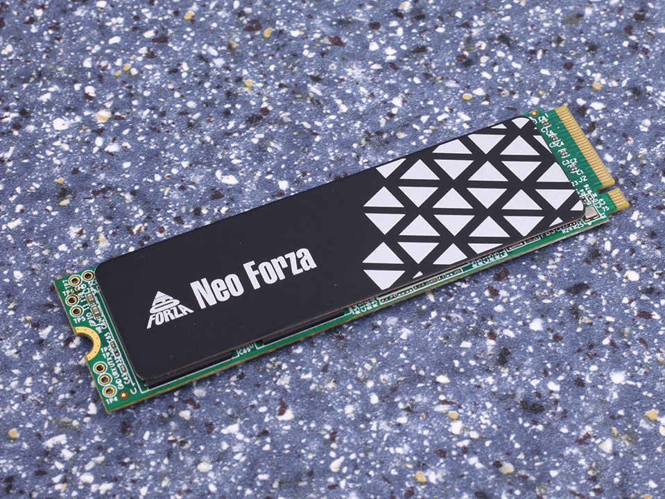

The drive uses the M.2 2280 form factor, which makes it 22 mm wide and 80 mm long.
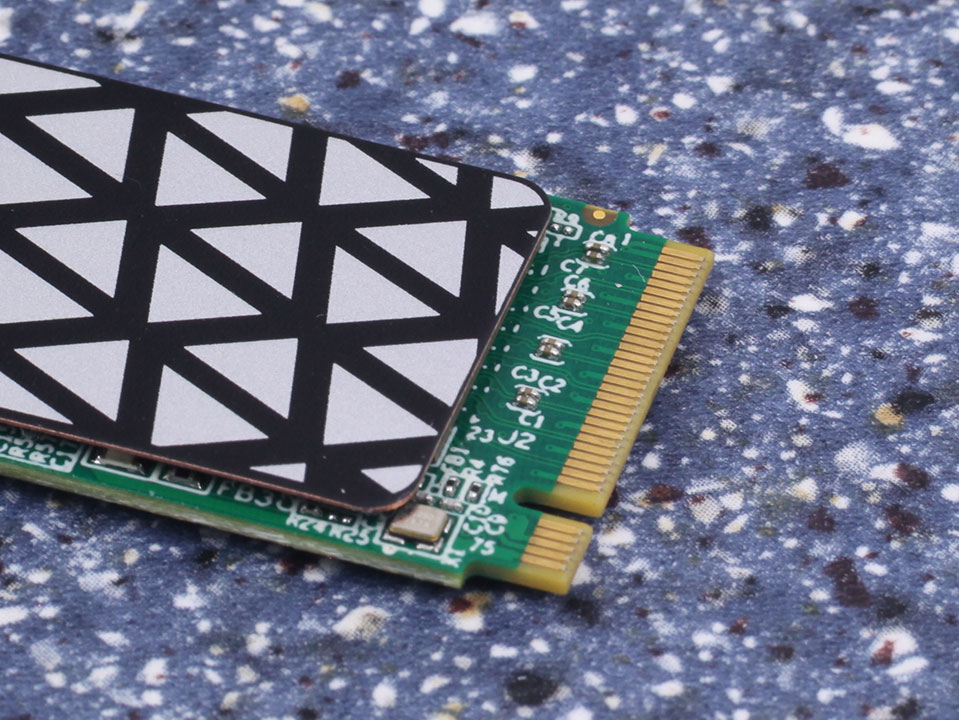
While most other M.2 NVMe SSDs transfer data over the PCI-Express 3.0 x4 interface, the Neo Forza NFP400 Series connects to the host system over a PCI-Express 4.0 x4 interface, which doubles the theoretical bandwidth.

On the top side of the SSD, Neo Forza installed this copper foil. It's an easy way to reduce SSD temperatures without a bulky heatsink.


On the PCB, you'll find the controller, four flash chips, and two DRAM chips.
Chip Component Analysis

The Innogrit IG5236 is the company's first controller to support PCI-Express 4.0. It uses eight channels to maximize transfer rates and is fabricated on a 12 nm process at TSMC Taiwan.

The four 128-layer 3D TLC flash chips are made by YMTC, a Chinese NAND maker that is government-backed. YMTC has an exclusive 3D die-stacking technology called Xtacking, which enables them to claim the "3D TLC" title, more about the tech here. Basically, the NAND storage array is manufactured on a die separate to the CMOS control logic die. In manufacturing, both dies are stacked with vertical interconnections. Obviously, this requires an extremely high degree of precision, but yields great density.
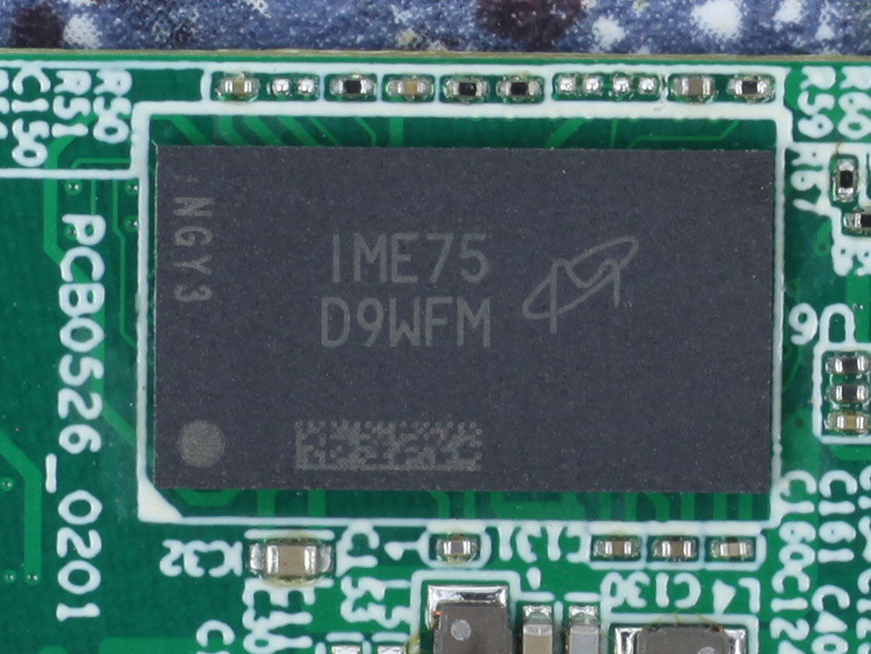
Two Micron DDR4-3200 chips provide a total of 2 GB of fast DRAM storage for the controller to store the mapping tables.
May 12th, 2024 17:57 EDT
change timezone
Latest GPU Drivers
New Forum Posts
- Which Audio System Would you Choose and Why? (6)
- Alphacool 280 xt45 Radiator repair (12)
- Air makes its way from the reservoir into the radiator. (37)
- Purchased an AX1200i PSU as part of some forward planning, what tier is this PSU? (55)
- Regular frametime spikes in all games (8)
- LOL ASUS says this is $200 in repair, Steve from gamers Nexus smokes ASUS, Steam Deck til I die boys!!!! (76)
- How to install nvidia driver for rtx3080 on windows 1709? (65)
- Xeon Owners Club (8703)
- How to optimize my PC by overclocking my system (5)
- I don't think Ryzen 9900x3d is just being announced next month, I think it's launching next month. (66)
Popular Reviews
- ZMF Caldera Closed Planar Magnetic Headphones Review
- ThundeRobot ML903 NearLink Review
- Corsair MP700 Pro SE 4 TB Review
- Bykski CPU-XPR-C-I CPU Water Block Review - Amazing Value!
- CHERRY XTRFY M64 Pro Review
- Upcoming Hardware Launches 2023 (Updated Feb 2024)
- ASRock NUC BOX-155H (Intel Core Ultra 7 155H) Review
- AMD Ryzen 7 7800X3D Review - The Best Gaming CPU
- Corsair iCUE Link RX120 RGB 120 mm Fan Review
- ASUS Radeon RX 7900 GRE TUF OC Review
Controversial News Posts
- Intel Statement on Stability Issues: "Motherboard Makers to Blame" (266)
- AMD to Redesign Ray Tracing Hardware on RDNA 4 (219)
- Windows 11 Now Officially Adware as Microsoft Embeds Ads in the Start Menu (171)
- NVIDIA to Only Launch the Flagship GeForce RTX 5090 in 2024, Rest of the Series in 2025 (147)
- Sony PlayStation 5 Pro Specifications Confirmed, Console Arrives Before Holidays (119)
- AMD's RDNA 4 GPUs Could Stick with 18 Gbps GDDR6 Memory (114)
- AMD Hits Highest-Ever x86 CPU Market Share in Q1 2024 Across Desktop and Server (108)
- AMD Ryzen 9 7900X3D Now at a Mouth-watering $329 (104)