 7
NVIDIA GeForce 8600 & 8500 Preview Review
(7 Comments) »Introduction


Today NVIDIA announced their new mainstream GeForce 8 Series based on the new 80nm G84 and G86 GPUs.
The new line-up of GPUs actually conists of five different offerings. The 8600 GTS is the most powerful mainstream GPU, followed by the 8600 GT. There is also an 8500 GT, which will not feature a seperate SLI connector, but will be capable of the dual graphic card standard from NVIDIA using PCI-E transfers. The company will also be offering a GeForce 8300 GS and 8400 GS to OEMs only to integrate into systems.
Specifications
| 8800 GTX | 8800 GTS 640MB | 8800 GTS 320MB | 8600 GTS | 8600 GT | 8500 GT | |
| GPU | G80 | G80 | G80 | G84 | G84 | G86 |
| Transistors | 681 M | 681 M | 681 M | 289 M | 289 M | 210 M |
| GPU Process size | 90 nm | 90 nm | 90 nm | 80 nm | 80 nm | 80 nm |
| Shader Model | 4.0 | 4.0 | 4.0 | 4.0 | 4.0 | 4.0 |
| Pixel Shaders | 128 | 96 | 96 | 32 | 32 | 16 |
| Vertex Pipes | ||||||
| ROP (#) | 24 | 20 | 20 | 8 | 8 | 4 |
| Memory Interface | 384 bit | 320 bit | 320 bit | 128 bit | 128 bit | 128 bit |
| Memory Size | 768 MB | 640 MB | 320 MB | 256/512 MB | 256 MB | 256 MB |
| Memory Type | GDDR3 | GDDR3 | GDDR3 | GDDR3 | GDDR3 | DDR2 |
| Core Clock | 575 MHz | 500 MHz | 500 MHz | 675 MHz | 540 MHz | 450 MHz |
| Memory Clock | 900 MHz | 800 MHz | 800 MHz | 1000 MHz | 700 MHz | 400 MHz |
| Shader Clock | 1350 MHz | 1200 MHz | 1200 MHz | 1450 MHz | 1180 MHz | 900 MHz |
| Interface | PCI-E | PCI-E | PCI-E | PCI-E | PCI-E | PCI-E |
| Inital Price | $599 | $449 | $399 | $199-229 | $149-159 | $89-129 |
Looking at these specs, it seems like there is a very large difference between the 8800 based cards and the 8600 series. While the new mainstream cards only have 32 shaders and only 128 bit bandwith, they are clocked quite high. The high performance on single slot cooling is possible due to the 80nm prodcess and greatly reduced transistor count.
The Cards
The following pictures always show the GeForce 8600 GTS first, followed by the 8600 GT and the 8500 GT.


The GeForce 8600 GTS is the biggest card of the new bunch. The heatsink is the largest as well. Even though it is running at a very fast 675 MHz, it is cooled by a single slot solution. The 8600 GT heatsinkhas grown a bit when compared to the 7600 GT reference cooler. It now cools the memory chips, which was not the case with the 7600 GT. The 8500 GT uses a very traditional square heatsink with fan. While the reference design uses active cooling, we may see several passive implementations in retail.


When viewed from the back, the 8600 GTS has noticably more components than the smaller variants. Even though the 8600 GT uses the same PCB as the 7600 GT series, it does not feature as many components. Both the G84 based implementations have their heatsinks secured by screws, while the G86 based 8500 GT uses plastic push-pins.


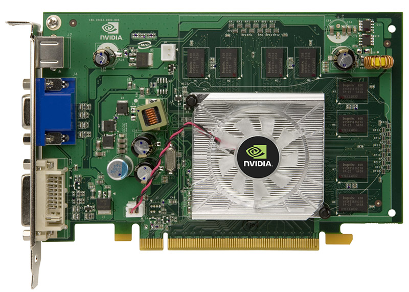
From the top the cards, the diffent cooler sizes become even more apparent. The other interesting part is the lack of an internal SLI connector on the 8500GT. This means, that even though you may run two of these in SLI, the performance gain will not be as large as with such a connection. If you look closely at the 8500 GT, the PCB actually features a white line around the memory as well. Some manufacturers may use such a cooler shape which cools the memory in combination with a fan.

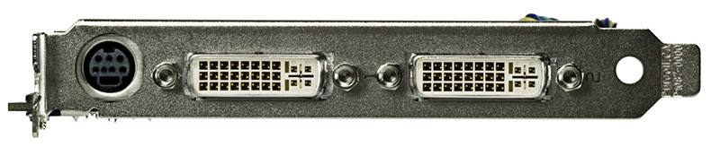

Both the 8600 GTS and 8600 GT brackets feature dual DVI connectord, as well as an S-Video output. The 8500 GT has a single D-SUB and DVI connector. All three cards have dual-link DVI connectors, which means that WQXGA (2560 × 1600) resolution is possible with a single card.


As mentioned before, the 8600 Series features the SLI connector, while the 8500 GT does not. Also note the overall size of the new mainstream parts, as these are much shorter. They should fit into any normal ATX or mATX case without having so sacrifice other features like hard drive bays.
Our Patreon Silver Supporters can read articles in single-page format.
Nov 15th, 2026 16:32 CST
change timezone
Latest GPU Drivers
New Forum Posts
- What are you playing? (26222)
- WarpCoreBench scores! (51)
- Asus Rog Maximus Z890 Extreme. (Various questions). (25)
- Power supply noise stops when I move the mouse (9)
- TPU's Nostalgic Hardware Club (22165)
- HP Office Jet 7740 Pro - Supply system problem with replacement cartridge (3)
- Recommendations Wanted - Affordable Enterprise SSD for Boot (9)
- Folding Pie and Milestones!! (10204)
- What can the FX 8320 do today? Here is the answer. (59)
- How do you get games for PC? (59)
Popular Reviews
- AMD Zen 6 Technical Deep Dive
- ASUS ROG Strix B850-I Gaming Wi-Fi7 W Review
- Corsair HX1000i Shift Crystal Review
- Upcoming Hardware Launches 2027 (Updated Nov 2026)
- Montech King 95 3D PRO Review
- NZXT C1200 Platinum Review
- NZXT H7 RGB+ Review
- NZXT H5 Review
- Phantom Blade Zero Performance Benchmark Review - 35 GPUs Tested
- AMD Ryzen 7 9800X3D Review - The Best Gaming Processor
TPU on YouTube
Controversial News Posts
- NVIDIA Co-Founder and CEO Jensen Huang Officially Resigns (421)
- Open Letter Asking NVIDIA to Reinstate Jensen Huang Passes 115,000 Signatures (184)
- OpenAI CEO Argues Home PCs Waste the World's Limited DRAM Supply (152)
- NVIDIA Launches Investigation Into Jensen Huang's Relationship With Suspected Chinese Spy (136)
- Intel "Raptor Lake Next" 16-Core and 20-Core CPUs Surface (130)
- Legendary Game Studio BioWare Shuts Down Following EA Layoffs (104)
- Dell CEO Says the Memory Shortage Will Get Worse in 2027 (95)
- NVIDIA GeForce RTX 50-Series Scheduled for up to $500 Price Hike This Week (89)