 61
61
NVIDIA GeForce Ampere Architecture, Board Design, Gaming Tech & Software
Raytracing & Tensor Core Improvements »GeForce Ampere Architecture

"Ampere" represents the 2nd generation of NVIDIA's GeForce RTX technology. Real-time raytracing made its debut in the consumer graphics segment ahead of its time, as it was believed to be too compute-intensive even with vast numbers of programmable shader cores. NVIDIA RTX addressed this by introducing a new raster+raytracing hybrid where much of the 3D scene is rendered by traditional raster graphics and select elements that benefit from RT are ray-traced. To do even this, NVIDIA had to develop innovations that minimize the number of required rays for raytracing, by relying heavily on AI-based de-noising. It hence required development of purpose-built (and sometimes fixed-function) hardware, such as RT cores, which process BVH and intersections, and tensor cores, which accelerate the matrix multiplications used in AI neural nets.
With "Ampere," we see the introduction of newer streaming multiprocessors—the main programmable shader muscle of NVIDIA GPUs—and the company's 2nd generation RT core and 3rd generation tensor core (tensor cores predate "Turing" and were introduced with "Volta"). The key drive behind the three is not just a generational improvement in raster performance, but also a reduction of the performance impact with RTX. The first wave of NVIDIA GeForce Ampere graphics cards consists of the GeForce RTX 3080, being offered as a flagship gaming graphics card at $700, and the halo-segment RTX 3090, at $1,500 and targeting enthusiasts. It comes as a surprise that both cards are based on variants of the same "GA102" silicon, as NVIDIA hasn't based its GeForce RTX 3080 card on a smaller silicon.
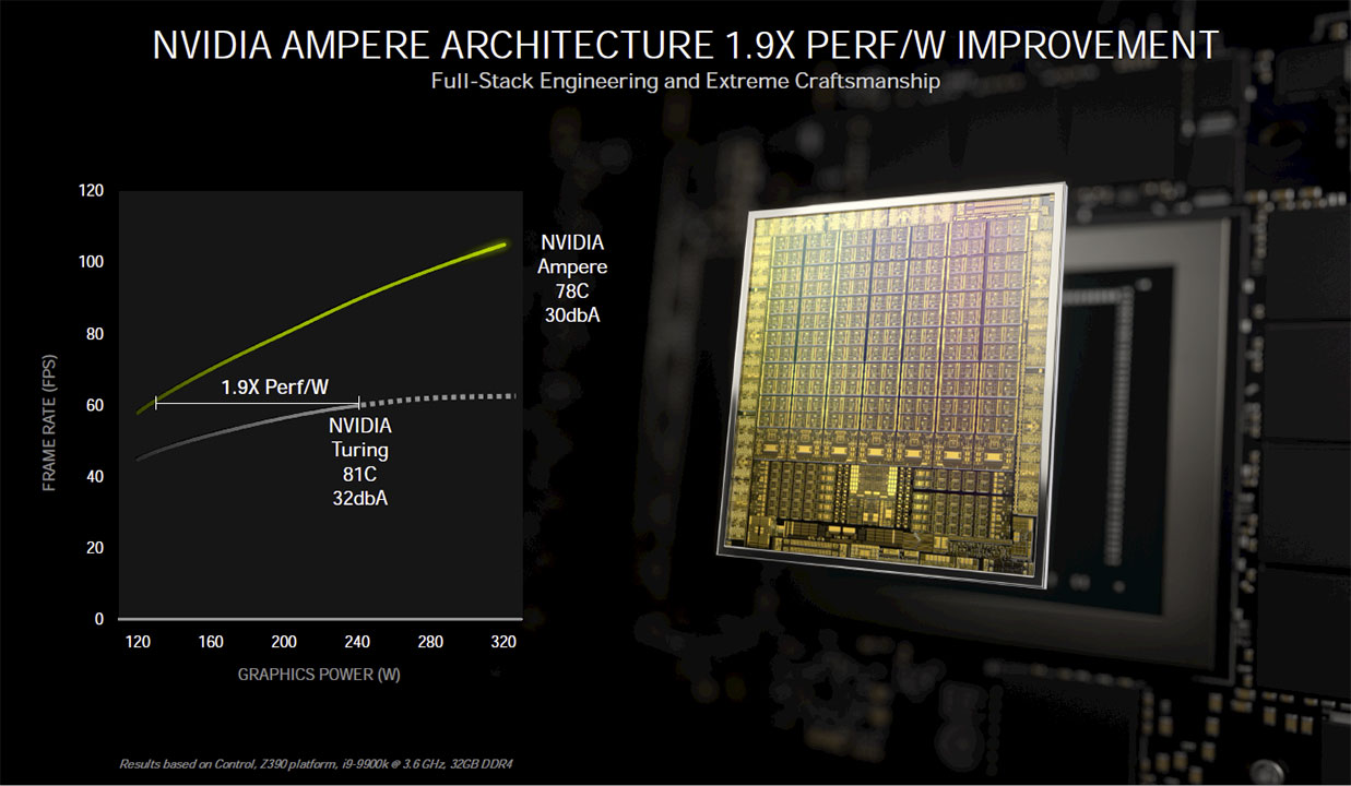
A dividend of the switch to 8 nm would perhaps be a massive gain in iso-power, which NVIDIA can use to dial up performance, directly impacting performance/watt. NVIDIA claims a massive 90% increase in performance/watt, so there's more to these cards than their apparent steep increases in typical board power.
NVIDIA GA102 Silicon
NVIDIA's GA102 chip is built on the 8 nanometer "8N" silicon fabrication node by Samsung. This node offers comparable transistor densities and iso-power to TSMC N7-class nodes, on which NVIDIA is making the A100 Tensor Core processor. The silicon features a gargantuan 28 billion transistors, and in its RTX 3080 trim offers raw compute throughput of up to 30 TFLOPs FP32, up to 58 ray-tracing TFLOPs, and up to 238 tensor TFLOPs.
Above is an architecture block diagram of the GA102 as implemented on the RTX 3080, which we created ourselves because the block diagram provided by NVIDIA is a simplified version. GA 102 has 8,704 CUDA cores spread across 68 streaming multiprocessors (SM), a staggering 183% increase in purely on-paper numerical terms over the RTX 2080 Super. This coupled with IPC improvements at the SM level works out to a massive 172% increase in FP32 throughput compared to the RTX 2080 Super (11 TFLOPs vs. 30 TFLOPs). Groups of two SMs, called texture processing clusters (TPC), remain the smallest segmentation unit of the Ampere architecture. The RTX 3080 features 34 TPCs (68 SMs) across six graphics processing clusters (GPCs).
At the outermost level, the GA102—as implemented on RTX 3080—features a PCI-Express 4.0 x16 host interface, the GigaThread which dispatches and coordinates work among the GPCs, an L2 (last-level) cache that serves as town-square for the GPCs, and a 320-bit wide GDDR6X memory interface. On the RTX 3090, this memory interface is broadened to 384-bit, and there are 41 TPCs spread across a larger number of GPCs. The RTX 3080 lacks an NVLink multi-GPU interface, while the RTX 3090 has it. NVIDIA changed the NVLink connector for space savings on the PCB (more on this later).

Here's the block diagram of the GA102 silicon as implemented on the RTX 3090. It has the full 384-bit wide memory interface of the GA102 enabled, along with all its GPCs, but one TPC (two SMs) is cut out for a better harvesting margin. With 82 SMs enabled, each with 128 CUDA cores, the RTX 3090 reaches its magic 10,000+ (10,490) CUDA core count. Another component not available on the RTX 3080 is the chip's NVLink interface. With each new generation, NVIDIA has been retreating SLI to higher segments in its product stack since multi-GPU is a dying technology and only enthusiasts chasing benchmark leaderboards would want to use it. Those after leaderboard rep would invest in the most expensive GPU anyway. SLI is rapidly fading away from the gamer's mind space.
The new Ampere SM

The streaming multiprocessor (SM) is where the bulk of NVIDIA's engineering effort has been directed. This is the key number-crunching component of the GPU. NVIDIA claims that the Ampere SM has double the compute muscle of the Turing SM. We still begin with four warp schedulers that stage workloads for the SIMD components, but each sub-unit now has 32 FP32 CUDA cores. Out of these, 16 can perform concurrent FP32+INT32 math operations.
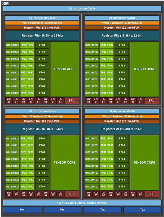
This is unlike the Ampere SM (pictured above for comparison) on the A100 Tensor Core scalar processor, which features sixteen FP32 and INT32 cores, each, and eight FP64 (double-precision) cores. Each sub-unit further has a 3rd generation tensor core, four load-store units, and a register file. Four such sub-units add up to 128 FP32 CUDA cores on the GeForce Ampere SM, of which 64 can handle concurrent INT32+FP32 ops. Each SM features one 2nd generation RT core, a 128 KB L1 data cache, and four TMUs. Thanks to a new data path, the GeForce Ampere SM features double the FP32 performance, or 128 fused multiply-add (FMA) ops per clock. The 2nd generation RT core supposedly offers double the triangle intersection rates over the previous generation, while the new 3rd generation tensor core offers double the math throughput with the leverage on high sparsity introduced with Ampere.
GDDR6X Memory

From what we gather, NVIDIA paired up with Micron Technology to develop GDDR6X, which seems to be an NVIDIA-exclusive memory technology. GDDR6X builds on JEDEC standard GDDR6 by taking advantage of multi-level PAM4 (pulse amplitude modulation 4) physical layer signaling, which makes it possible to transmit four possible values per cycle. Remember when they told you binary is just two values, "on" or "off", "one" and "zero". Well, this has changed—PAM4 transmits at four different voltage levels to pack double the data into each clock cycle.

The challenge is to avoid signal degradation so that the voltage levels can still clearly be told apart. It's kinda easy with "on" and "off", but distinguishing four different signal levels is more difficult, which is why new encoding is used for the data. Instead of transmitting the raw values directly, a 0 as no voltage and a 3 as maximum voltage every time, the MTA (maximum transition avoidance) coding scheme picks voltage levels depending on the previous level, so that the difference from clock-to-clock is not a full voltage swing.
Last but not least, NVIDIA improved their training algorithm in the memory controller—it is now more robust. It will now retrain from time to time and can adapt to changes in the environment, like temperature or EMI interference.
NVIDIA has been able to increase data rates because of it, up to 19.5 Gbps for the RTX 3090 and 19 Gbps for the RTX 3080. For the RTX 3090, this results in memory bandwidths approaching 940 GB/s, close to what can be accomplished with much pricier memory solutions, such as 4096-bit HBM2.
Apr 26th, 2024 10:11 EDT
change timezone
Latest GPU Drivers
New Forum Posts
- Old high quality PSU, or semi-old mid-quality PSU? (2)
- Secure boot already open help (8)
- What are you playing? (20540)
- Horizontal black lines popping up on my screen? (13)
- Alphacool CORE 1 CPU block - bulging with danger of splitting? (26)
- What's your latest tech purchase? (20351)
- The Official Linux/Unix Desktop Screenshots Megathread (698)
- Which new games will you be buying? (321)
- GoDeal24 Windows 11 Pro 32-bit! (3)
- Best SSD for system drive (86)
Popular Reviews
- HYTE THICC Q60 240 mm AIO Review
- Alienware Pro Wireless Gaming Keyboard Review
- MOONDROP x Crinacle DUSK In-Ear Monitors Review - The Last 5%
- Upcoming Hardware Launches 2023 (Updated Feb 2024)
- Intel Core i5-14600K Review - Impressive OC Potential
- Thermalright Phantom Spirit 120 EVO Review
- ASUS Radeon RX 7900 GRE TUF OC Review
- FiiO K19 Desktop DAC/Headphone Amplifier Review
- RTX 4090 & 53 Games: Ryzen 7 5800X vs Ryzen 7 5800X3D Review
- NVIDIA RTX 4090: 450 W vs 600 W 12VHPWR - Is there any notable performance difference?
Controversial News Posts
- Windows 11 Now Officially Adware as Microsoft Embeds Ads in the Start Menu (123)
- Sony PlayStation 5 Pro Specifications Confirmed, Console Arrives Before Holidays (117)
- NVIDIA Points Intel Raptor Lake CPU Users to Get Help from Intel Amid System Instability Issues (106)
- AMD "Strix Halo" Zen 5 Mobile Processor Pictured: Chiplet-based, Uses 256-bit LPDDR5X (101)
- US Government Wants Nuclear Plants to Offload AI Data Center Expansion (98)
- AMD's RDNA 4 GPUs Could Stick with 18 Gbps GDDR6 Memory (90)
- Developers of Outpost Infinity Siege Recommend Underclocking i9-13900K and i9-14900K for Stability on Machines with RTX 4090 (85)
- Windows 10 Security Updates to Cost $61 After 2025, $427 by 2028 (84)