 341
341
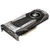
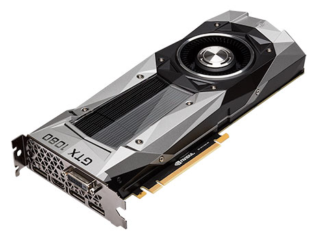
NVIDIA GeForce GTX 1080 8 GB Review
(341 Comments) »Introduction
NVIDIA is shaping up to be the most consistent chipmaker in the industry when it comes to per-generation performance and energy efficiency gains. Over the past three generations, spread across the past four years, the company dedicated vast R&D resources to developing increasingly more energy efficient GPUs. The 2012 "Kepler," followed by the 2014 "Maxwell" architectures, provided performance and energy efficiency leaps that do the word "leap" justice. At its recent GeForce 1080 "Pascal" unveiling, the company claimed to shatter all previous performance-to-wattage records, promising another leap in performance and efficiency.
The GeForce "Pascal" architecture debuted this April at NVIDIA's GTC event, driving the company's Tesla P100 HPC processor based on the massive GP100 silicon. The architecture's consumer-graphics debut was earlier this month, in the form of the GeForce GTX 1080, reviewed today, and the GeForce GTX 1070. The GTX 1080 will hit shelves on May 27th, with the GTX 1070 following closely on June 10th.
The GeForce GTX 1080 logically succeeds the GeForce GTX 980 and is priced not too far apart from its predecessor. It will launch at $599 where the GTX 980 debuted at $549. NVIDIA, however, is positioning it as a premium part since it's supposedly faster than any currently available single-GPU card. The company has hence come up with a clever marketing tactic.
Historically, reference-design cards set the baseline launch price for SKUs. This time around, NVIDIA is making its partners sell the reference-design card at $699 (higher than the launch prices of the GTX 980 Ti, GTX 780 Ti, etc.). The company is sub-branding this SKU as the "Founders Edition." Since this also happens to be the only GTX 1080 card designed entirely by NVIDIA, it's the card we are reviewing today. Custom-design cards will start at $599, but this is really a "suggested" price by NVIDIA to its partners. Adding meaty cooling solutions and custom VRM designs to the mix could easily push prices way above the $599 mark and perhaps even close to the $699 "Founders Edition" price, which could have partners take that as the baseline instead.
The GeForce GTX 1080 is based on NVIDIA's "Pascal" architecture. This architecture sees the streaming multiprocessors (SMs), the indivisible subunits of an NVIDIA GPU, get even more dedicated components, which increases their performance. NVIDIA claims to have "meticulously" designed the GPU architecture to be as energy efficient as possible given the silicon fab node and is leveraging the 16 nm FinFET node at TSMC for "Pascal."
The GTX 1080 features more CUDA cores than its predecessor – 2560 vs. 2048. It features even more TMUs (160 vs. 128) and, at 8 GB, double the memory. Memory technology sees a major update with NVIDIA's adoption of the GDDR5X memory standard. The memory is clocked at a staggering 10 GHz effective, at which speed the GPU has 320 GB/s of memory bandwidth over a 256-bit wide memory interface. Such bandwidths were only possible with 384-bit or 512-bit GDDR5 memory interfaces. First-generation HBM being restricted to 4 GB, HBM2 not being readily available, and HBM-class stacked memory being more expensive to deploy (using on-chip silicon substrates) could have contributed to NVIDIA's decision to go with GDDR5X for the GeForce GTX 1080.
In this review, we're testing a GeForce GTX 1080 reference-design graphics card, which NVIDIA is marketing as the "Founders Edition" at $699. This will be the price we will use in our primary price/performance calculation, although we did add a $599 price/performance data point as a reference.
| GeForce GTX 970 | Radeon R9 290X | Radeon R9 390X | GeForce GTX 780 Ti | GeForce GTX 980 | Radeon R9 Fury | Radeon R9 Fury X | GeForce GTX 980 Ti | GeForce GTX Titan X | Radeon R9 295X2 | GeForce GTX 1080 | |
|---|---|---|---|---|---|---|---|---|---|---|---|
| Shader Units | 1664 | 2816 | 2816 | 2880 | 2048 | 3584 | 4096 | 2816 | 3072 | 2x 2816 | 2560 |
| ROPs | 56 | 64 | 64 | 48 | 64 | 64 | 64 | 96 | 96 | 2x 64 | 64 |
| Graphics Processor | GM204 | Hawaii | Hawaii | GK110 | GM204 | Fiji | Fiji | GM200 | GM200 | 2x Hawaii | GP104 |
| Transistors | 5200M | 6200M | 6200M | 7100M | 5200M | 8900M | 8900M | 8000M | 8000M | 2x 6200M | 7200M |
| Memory Size | 4 GB | 4 GB | 8 GB | 3 GB | 4 GB | 4 GB | 4 GB | 6 GB | 12 GB | 2x 4 GB | 8 GB |
| Memory Bus Width | 256 bit | 512 bit | 512 bit | 384 bit | 256 bit | 4096 bit | 4096 bit | 384 bit | 384 bit | 2x 512 bit | 256 bit |
| Core Clock | 1051 MHz+ | 1000 MHz | 1050 MHz | 876 MHz+ | 1126 MHz+ | 1000 MHz | 1050 MHz | 1000 MHz+ | 1000 MHz+ | 1018 MHz | 1607 MHz+ |
| Memory Clock | 1750 MHz | 1250 MHz | 1500 MHz | 1750 MHz | 1750 MHz | 500 MHz | 500 MHz | 1750 MHz | 1750 MHz | 1250 MHz | 1251 MHz |
| Price | $285 | $280 | $380 | $390 | $400 | $470 | $620 | $550 | $1150 | $620 | $599 / $699 |
Architecture
The GeForce GTX 1080 is based on NVIDIA's second biggest GPU based on the "Pascal" architecture, the GP104. The biggest GPU is the GP100 driving the Tesla P100 HPC processor. The GP104 succeeds the GM204 (GTX 980, GTX 970), and despite having a smaller die at 314 mm² when compared to the 398 mm² of the GM204, it does feature significantly higher transistor counts at 7.2 billion when compared to the 5.2 billion of the GM204. This is due to NVIDIA's big move to the 16 nm FinFET process.
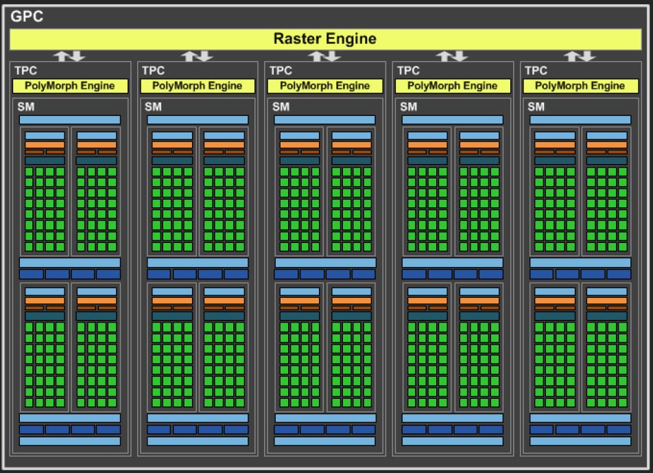

With each successive architecture since "Fermi," NVIDIA has been enriching the streaming multiprocessor (SM) by adding more dedicated resources and reducing shared resources within the graphics processing cluster (GPC), which leads to big performance gains. The story continues with "Pascal." Like the GM204 before it, the GP104 features four GPCs, super-specialized subunits of the GPU that share the PCI-Express 3.0 x16 host interface and the 256-bit GDDR5X memory interface through eight controllers. These controllers support both GDDR5X and GDDR5 memory, and the upcoming GeForce GTX 1070 is expected to feature 7 Gbps GDDR5 memory instead of the 10 Gbps GDDR5X on the GTX 1080.
Workload across the four GPCs is shared by the GigaThread Engine cushioned by 2 MB of cache. Each GPC holds five streaming multiprocessors (SMs), which is an increase from the four SMs each GPC held on the GM204. The GPC shares a raster engine between these five SMs. The "Pascal" streaming multiprocessor features a 4th generation PolyMorph Engine, a component for key render setup operations. With "Pascal," the PolyMorph Engine includes specialized hardware for the new Simultaneous MultiProjection feature. Each SM also holds a block of eight TMUs.
Each SM continues to feature 128 CUDA cores. The GP104 hence features a total of 2,560 CUDA cores. Other vital specifications include 160 TMUs and 64 ROPs. NVIDIA claims to have worked on a new GPU internal circuit design and board channel paths to facilitate significantly higher clock speeds than what the GM204 is capable of. The GeForce GTX 1080 ships with a staggering 1607 MHz GPU clock speed for a maximum GPU Boost frequency of 1733 MHz. At its launch event earlier this month, NVIDIA demonstrated a 2.1 GHz GPU overclock on the reference-design board with stock air-cooling, so we know this GPU likes to overclock.

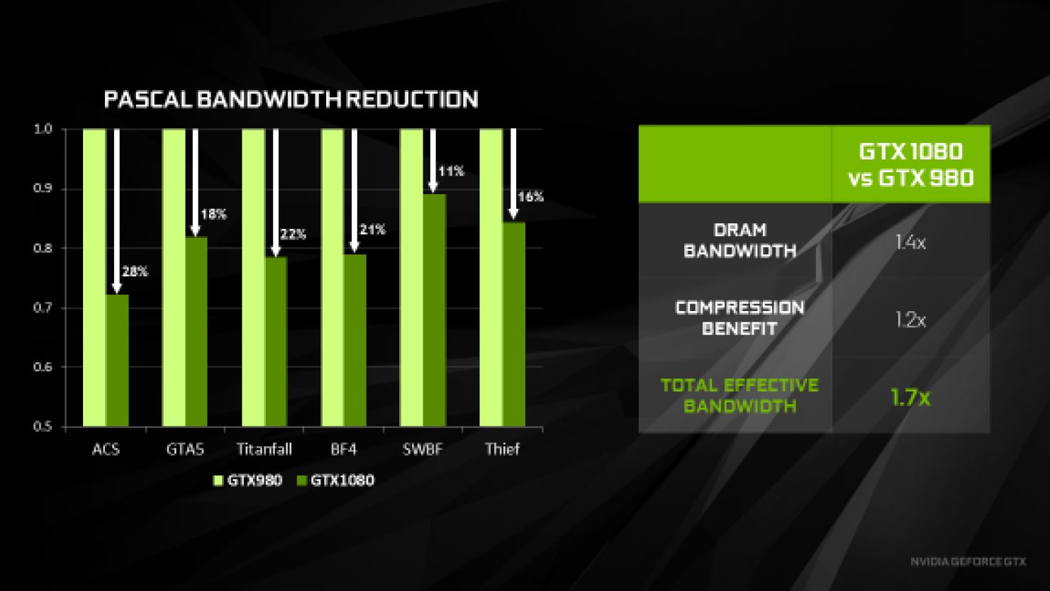
The GeForce GTX 1080 is the first graphics card to use the new GDDR5X memory standard. The interface enables effective data-rates that are as high as 14 GHz, and although it has many bare-metal specifications in common with GDDR5, minimizing R&D for its implementation, the memory chip design is improved with higher pin counts to support these higher data-rates. The memory is clocked at an effective 10 GHz. Over a 256-bit memory interface, this works out to a memory bandwidth of 320 GB/s NVIDIA has also optimized the usage of with more advanced 4th generation lossless Delta Color Compression. The best-case scenario has Delta Color Compression provide an "effective" memory bandwidth uplift of 20 percent, which results in 384 GB/s.
The "Pascal" architecture supports Asynchronous Compute as standardized by Microsoft. It adds to that with its own variation of the concept with "Dynamic Load Balancing."


The New Age of Multi-GPU
With Microsoft DirectX 12 introducing a standardized mixed multi-GPU mode in which a DirectX 12 (and above) 3D app can take advantage of any number and types of GPUs as long as they support the API features needed by the app, multi-GPU has changed forever. Instead of steering its GPU lineup toward that future, NVIDIA has spent some R&D on its proprietary SLI technology. With increasing resolutions and refresh rates straining the bandwidth of display connectors and inter-GPU communication in multi-GPU modes, NVIDIA decided that SLI needs added bandwidth. One way it saw to doing so was to task both SLI contact points on the graphics card in a 2-way configuration. Enter the SLI HB (high-bandwidth) bridge, a rigid SLI bridge that comes in 1U, 2U, and 3U slot spacings for a link between two GeForce "Pascal" graphics cards along both their SLI "fingers" (contact points). This allows a SLI duo to more reliably render at such resolutions as 4K @ 60 Hz or 120 Hz, and 5K, or HDR-enabled resolutions. SLI could still work with a classic 2-way bridge at any resolution, but that could adversely affect performance upscaling, and the output won't be as smooth as with an SLI HB bridge. This also appears to be why NVIDIA discontinued official support for 3-way and 4-way SLI.

The GTX 1080 still supports 3-way and 4-way SLI over the classic bridges that come with motherboards, but you would have to obtain a special software key from NVIDIA and would rely on your game/benchmark developers to optimize their apps for 3-way/4-way SLI. NVIDIA's regular driver updates will likely only optimize for 2-way SLI. Enthusiasts wanting to use 3-way or 4-way SLI would download an app from an upcoming "Enthusiast Key" website, run the app, and generate a software key signature for their hardware to unlock 3-way and 4-way SLI in NVIDIA's Control Panel. NVIDIA "Pascal" GPUs do support Microsoft DirectX 12's multi-display adapter (MDA) mode, but NVIDIA will not provide game-specific optimizations through driver updates for MDA. That would become the game developer's responsibility. The same applies to "explicit" LDA (linked display adapter).
New Display Connectors
The "Pascal" architecture features DisplayPort 1.4 even though it's only certified for up to DisplayPort 1.2. You can enjoy all the features of DisplayPort 1.3 and 1.4 just fine, such as HDR metadata transport. The GPU also supports HDMI 2.0b, the latest HDMI standard with support for HDR video. In the entire course of its presentation, NVIDIA did not mention whether "Pascal" supports VESA AdaptiveSync, which AMD is co-branding as FreeSync. All you need for it to work is a GPU that supports HDMI 2.0a or DisplayPort 1.2a (which are both satisfied by NVIDIA supporting HDMI 2.0b and DisplayPort 1.4). All that's needed is support on the driver's side. The GeForce GTX 1080 features an HDMI 2.0b, a dual-link DVI-D, and three DisplayPort 1.4 connectors. The DVI connector lacks analog wiring, and, thus, the GTX 1080 lacks support for D-Sub monitors through dongles.Fast Sync

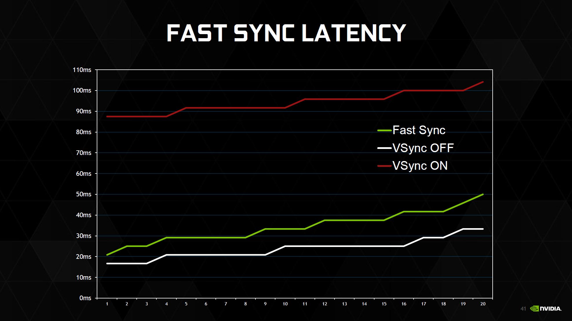
With each new architecture over the past three generations, NVIDIA toyed with display sync. With "Kepler," it introduced Adaptive V-Sync, by the time "Maxwell" came along, you had G-SYNC, and with "Pascal," the company is introducing a new feature called Fast Sync. NVIDIA states Fast Sync to be a low-latency alternative to V-Sync that eliminates frame-tearing (normally caused because the GPU's output frame-rate is above the display's refresh-rate) while letting the GPU render unrestrained from V-Sync, which reduces input latency. This works by decoupling the display pipelines and render output, which makes temporarily storing excessive frames that have been rendered in the frame buffer possible. The result is an experience with low input-lag (from V-Sync "off") and no frame-tearing (from V-Sync "on"). You will be able to enable Fast Sync for a 3D app by editing its profile in NVIDIA Control Panel; simply force Vertical Sync mode to "Fast."
Our Patreon Silver Supporters can read articles in single-page format.
Apr 26th, 2024 11:49 EDT
change timezone
Latest GPU Drivers
New Forum Posts
- im new to throttelstop and i think i messed it up by copying others any hints would be very much aprreciated (4)
- The TPU UK Clubhouse (24787)
- Cs2 Freezing in Rx 580 (5)
- Ghost of Tsushima PC Port !!!! (15)
- The Official Linux/Unix Desktop Screenshots Megathread (699)
- Red Dead Redemption using emu (4)
- Meta Horizon OS (21)
- Old high quality PSU, or semi-old mid-quality PSU? (3)
- Secure boot already open help (8)
- What are you playing? (20540)
Popular Reviews
- HYTE THICC Q60 240 mm AIO Review
- MOONDROP x Crinacle DUSK In-Ear Monitors Review - The Last 5%
- Alienware Pro Wireless Gaming Keyboard Review
- Upcoming Hardware Launches 2023 (Updated Feb 2024)
- Thermalright Phantom Spirit 120 EVO Review
- ASUS Radeon RX 7900 GRE TUF OC Review
- FiiO K19 Desktop DAC/Headphone Amplifier Review
- RTX 4090 & 53 Games: Ryzen 7 5800X vs Ryzen 7 5800X3D Review
- NVIDIA RTX 4090: 450 W vs 600 W 12VHPWR - Is there any notable performance difference?
- Sapphire Radeon RX 7900 GRE Pulse Review
Controversial News Posts
- Windows 11 Now Officially Adware as Microsoft Embeds Ads in the Start Menu (125)
- Sony PlayStation 5 Pro Specifications Confirmed, Console Arrives Before Holidays (117)
- NVIDIA Points Intel Raptor Lake CPU Users to Get Help from Intel Amid System Instability Issues (106)
- AMD "Strix Halo" Zen 5 Mobile Processor Pictured: Chiplet-based, Uses 256-bit LPDDR5X (101)
- US Government Wants Nuclear Plants to Offload AI Data Center Expansion (98)
- AMD's RDNA 4 GPUs Could Stick with 18 Gbps GDDR6 Memory (92)
- Developers of Outpost Infinity Siege Recommend Underclocking i9-13900K and i9-14900K for Stability on Machines with RTX 4090 (85)
- Windows 10 Security Updates to Cost $61 After 2025, $427 by 2028 (84)