 225
225
NVIDIA GeForce GTX 980 4 GB Review
(225 Comments) »Introduction
NVIDIA is doing the scientific community a great service by code-naming its GPU architectures after pioneering physicists. "Kepler" became synonymous with the GeForce GTX 680 launch back in 2012; and although it got its debut with the mid-range GeForce GTX 750 Ti earlier this year, "Maxwell", NVIDIA's latest GPU architecture, is really beginning to unravel with the new GeForce GTX 980 and GTX 970 we are reviewing today.

The development cycle of GPUs isn't too different from that of CPUs. A new GPU architecture is introduced every two or so years, facilitated by a new silicon fab process, which allows designers to cram in more transistors, to up performance. The common foundry partner for both NVIDIA and AMD, TSMC, threw a spanner into the workings of this cycle when news broke of delays in the implementation of its 20 nanometer manufacturing node, successor to the 28 nm node on which NVIDIA's GeForce Kepler and AMD's "Volcanic Islands" families of GPUs were built. NVIDIA probably had to redesign the performance-segment GPU based on its swanky new "Maxwell" GPU architecture for the existing 28 nm node. Its fruition is the GM204, the 5.2 billion transistor chip at the heart of the GeForce GTX 980 and GTX 970.
With the introduction of the GeForce GTX 980 and GTX 970, NVIDIA's product stack looks very similar to the way it did in 2012, in which the performance-segment GK104 went into making the GTX 680 and GTX 670, positioned as high-end parts because of their relatively higher performance to AMD's high-end chips at the time. Much like "Kepler" and GK104, "Maxwell" and GM204 boast leaps in performance-per-watt and overall performance. However, those two facets aren't Maxwell's only propositions. NVIDIA announced a bucket-list of innovations in consumer-graphics technologies, such as support for Microsoft's next-generation DirectX 12 API, Dynamic Super Resolution, Multi-Frame Sampled AA, Voxel Global Illumination, and VR Direct. Such is NVIDIA's confidence in the superiority of its "Maxwell" architecture, that it thinks a 28 nm chip with 165W TDP can outperform "Kepler" based chips on the same 28 nm process with a 50 percent higher TDP.

The GeForce GTX 980, hence, is NVIDIA's newest high-end single-GPU graphics card, by possible virtue of its performance. It is priced at US $549, which is $100 cheaper than the GeForce GTX 780 at launch, but $50 more than the GTX 680 at its launch. The GeForce GTX 970, on the other hand, is a high-performance offering priced at $329. With the introduction of these two, NVIDIA announced the discontinuation of the GeForce GTX 780 and GTX 770 from the product stack. The GTX 760 even sees a price-cut that puts it at $219. NVIDIA priced the GTX 980 to lock horns with AMD's R9 290X, and the GTX 970 is slotted to compete against the R9 290. Will they succeed?
| GeForce GTX 680 | GeForce GTX 780 | Radeon R9 290 | GeForce GTX 970 | Radeon R9 290X | Radeon HD 7990 | GeForce GTX Titan | GeForce GTX 780 Ti | GeForce GTX 980 | GeForce GTX 690 | Radeon R9 295X2 | |
|---|---|---|---|---|---|---|---|---|---|---|---|
| Shader Units | 1536 | 2304 | 2560 | 1664 | 2816 | 2x 2048 | 2688 | 2880 | 2048 | 2x 1536 | 2x 2816 |
| ROPs | 32 | 48 | 64 | 64 | 64 | 2x 32 | 48 | 48 | 64 | 2x 32 | 2x 64 |
| Graphics Processor | GK104 | GK110 | Hawaii | GM204 | Hawaii | 2x Tahiti | GK110 | GK110 | GM204 | 2x GK104 | 2x Hawaii |
| Transistors | 3500M | 7100M | 6200M | 5200M | 6200M | 2x 4310M | 7100M | 7100M | 5200M | 2x 3500M | 2x 6200M |
| Memory Size | 2048 MB | 3072 MB | 4096 MB | 4096 MB | 4096 MB | 2x 3072 MB | 6144 MB | 3072 MB | 4096 MB | 2x 2048 MB | 2x 4096 MB |
| Memory Bus Width | 256 bit | 384 bit | 512 bit | 256 bit | 512 bit | 2x 384 bit | 384 bit | 384 bit | 256 bit | 2x 256 bit | 2x 512 bit |
| Core Clock | 1006 MHz+ | 863 MHz+ | 947 MHz | 1051 MHz+ | 1000 MHz | 1000 MHz | 837 MHz+ | 876 MHz+ | 1126 MHz+ | 915 MHz+ | 1018 MHz |
| Memory Clock | 1502 MHz | 1502 MHz | 1250 MHz | 1750 MHz | 1250 MHz | 1500 MHz | 1502 MHz | 1750 MHz | 1750 MHz | 1502 MHz | 1250 MHz |
| Price | $340 | $420 | $370 | $330 | $460 | $1000 | $1000 | $590 | $550 | $1000 | $1000 |
Architecture
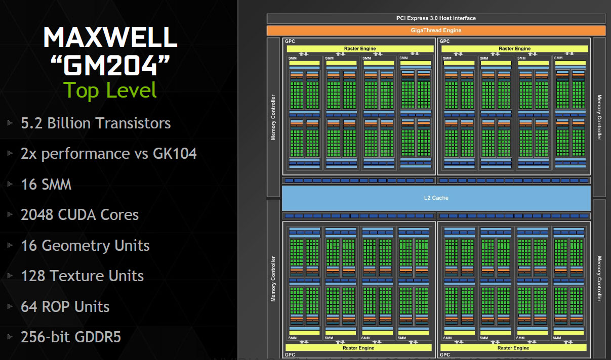
As we mentioned earlier, Maxwell was likely supposed to be built on the newer 20 nanometer node, but TSMC's delays in implementing it may have forced NVIDIA into redesigning it for the existing 28 nm process, which can be a disadvantage because the transistor counts and power budgets are based on a newer, smaller node. NVIDIA now had to make sure these work just as well on the existing node. GM204 crams a staggering 5.2 billion transistors into a die that measures 398 mm², and a package that's roughly the same size. It has 2 billion more transistors than the GK104 yet 1.9 billion transistors less than the GK110 on which its predecessor, the GTX 780, was built.


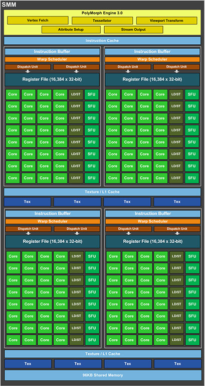
At the heart of the Maxwell architecture is a redesigned streaming multiprocessor (SMM), the tertiary subunit of the GPU. Variants of NVIDIA's GeForce GTX products are carved out by setting the number of SMM units at the chip's disposal. The GM204 has a similar component hierarchy as the GK104.
The chip begins with a PCI-Express 3.0 x16 bus interface, a 256-bit wide GDDR5 memory interface, and a display controller that supports as many as three Ultra HD displays, or five physical displays in total. This display controller introduces support for HDMI 2.0, which has enough bandwidth to drive Ultra HD displays at 60 Hz refresh rates. The controller is ready for 5K (5120x2880, four times the pixels as QuadHD). The 256-bit wide memory interface holds a standardized 4 GB of memory, with the bus clocked at 7.00 GHz on both the GTX 980 and GTX 970, which works out to a memory bandwidth of 224 GB/s. Don't let that worry you as NVIDIA is implementing a new lossless Delta color compression algorithm to make the most of the available memory bandwidth.
The GigaThread Engine splits workloads between four graphics processing clusters (GPCs). The L2 cache cushion transfers between these GPCs, and other components have been quadrupled in size. The GM204 ships with 2 MB of cache, compared to the 512 KB on the GK104. Each GPC holds four streaming multiprocessors (SMMs) and a common raster engine between them. Each SMX holds a third-generation PolyMorph Engine, a component that performs a host of rendering tasks, such as fetch, transform, setup, tessellation, and output. The SMX has 128 CUDA cores, the number-crunching components of NVIDIA GPUs, spread across four subdivisions with dedicated warp-schedulers, registers, and caches. NVIDIA claims the SMM to have two times the performance-per-watt figure of "Kepler" SMX units.


With four such 128-core SMMs per GPC, and four GPCs, the GM204 features 2,048 CUDA cores in all. Other vital specs include 128 texture memory units (TMUs) and 64 raster-operations units (ROPs). The ROP count is interesting as it has doubled over the GK104 and is greater than the 48 on the GM110. The third-generation Delta-color memory compression tech helps the chip make the most of its 224 GB/s memory bandwidth. It provides lossless compression, so textures will not feel washed out. With this tech in place, NVIDIA achieved savings of up to 29 percent in memory bandwidth usage; and so 7 Gbps memory "effectively" runs at 9.3 Gbps (although NVIDIA doesn't use "effective" bandwidth in its specs sheets).
GeForce Features
With each new architecture, NVIDIA introduces innovations in the consumer graphics space that go beyond simple feature-level compatibility with new DirectX versions. NVIDIA says GeForce GTX 980 and GTX 970 cards to be DirectX 12 cards, but exact feature levels and requirements have not been finalized by Microsoft, yet support for OpenGL 4.4 has also been added. OpenGL 4.4 adds a few new features through its GameWorks SDK that give game developers easy-to-implement visual features through existing APIs.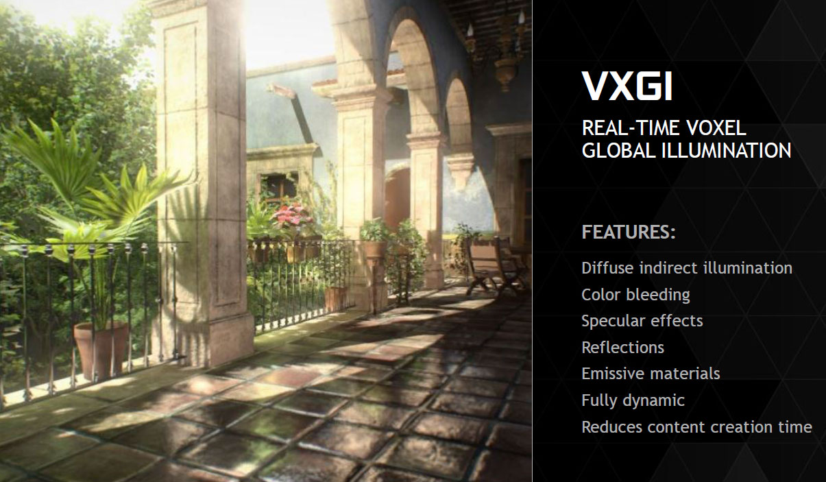
According to NVIDIA, the first and most important is VXGI, or real-time voxel global illumination. VGXI adds realism to the way light behaves with different surfaces in a 3D scene. VXGI introduces volume pixels, or voxels, a new 3D graphics component. These are pixels with built-in 3-dimensional data, so their interactions in 3D objects with light look more photo-realistic.
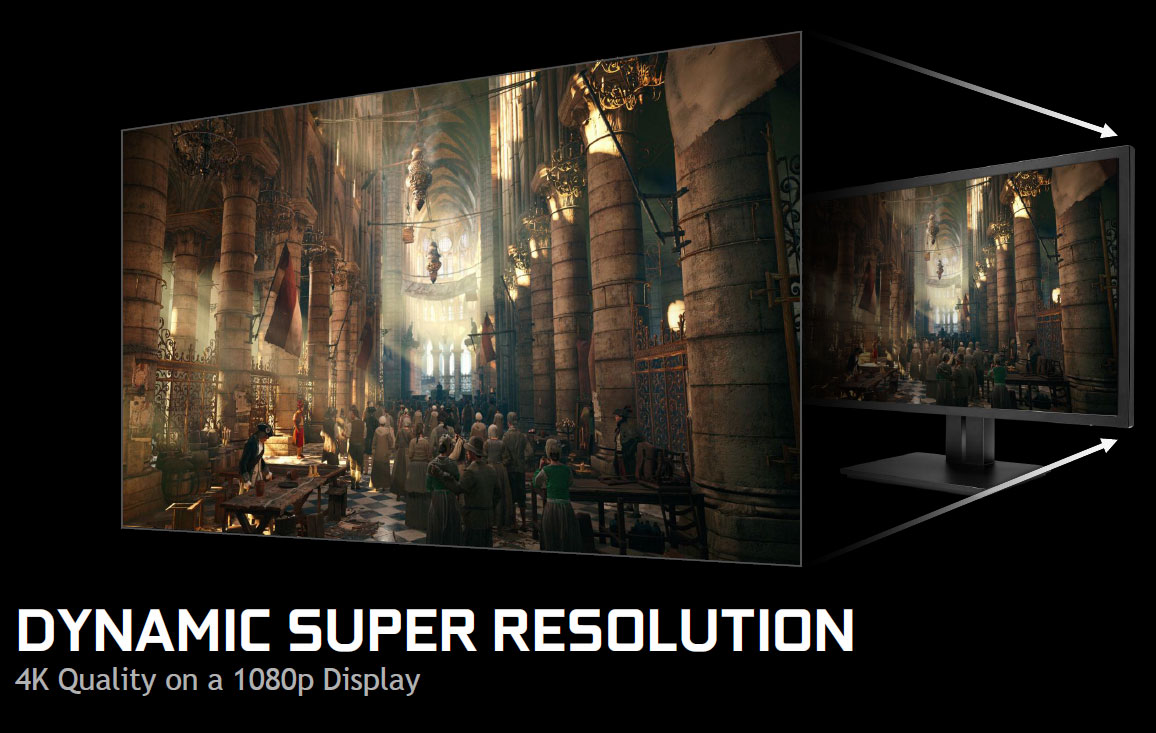

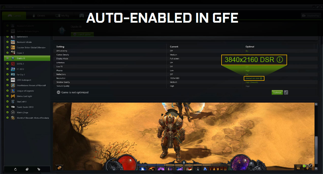
No new NVIDIA GPU architecture launch is complete without advancements in post-processing, particularly anti-aliasing. NVIDIA introduced an interesting feature called Dynamic Super Resolution (DSR), which it claims offers "4K-like clarity on a 1080p display". To us, it comes across as a really nice super-sampling AA algorithm with a filter.


Using GeForce Experience, you can enable DSR arbitrarily for 3D apps. The other new algorithm is MFAA (multi-frame sampled AA), which offers MSAA-like image quality at a deficit of 30 percent in performance. Using GeForce Experience, MFAA can hence be substituted for MSAA, perhaps even arbitrarily.


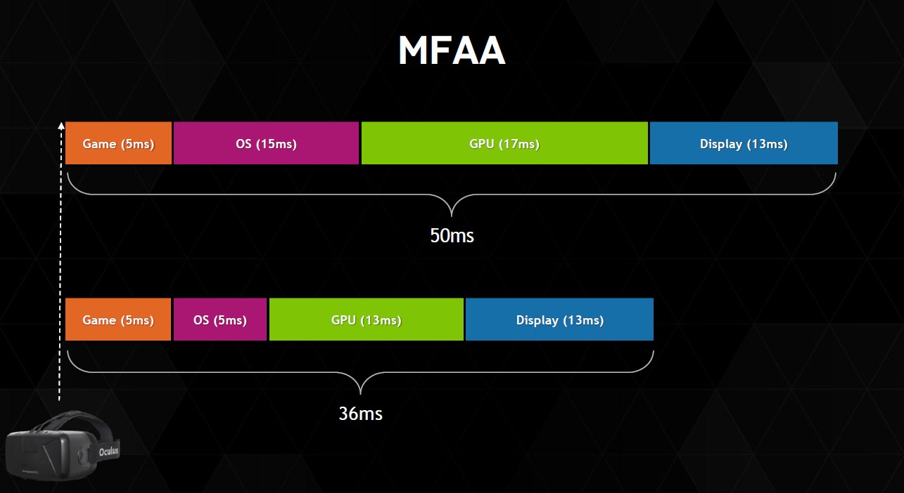
Moving on, NVIDIA introduced VR Direct, a technology designed for the reemerging VR headset market, due to the growing interest in Facebook's Occulus Rift VR headset. VR Direct is an API designed to reduce latency between the headset's input and the change on the display, governed by the principle that head movements are more rapid and unpredictable than pointing and clicking with a mouse.


To meet the need of a low-cost (performance cost), realistic hair- or grass-rendering technology, NVIDIA came up with Turf Effects. NVIDIA PhysX also got a much needed feature-set update that introduces new gas dynamics and fluid adhesion effects. Epic's Unreal Engine 4 will implement the technology.
GeForce Experience
With its GeForce 320.18 WHQL drivers, NVIDIA released the first stable version of GeForce Experience. The application simplifies the process of configuring a game and is meant for PC gamers who aren't well-versed in all the necessary technobabble required to get a game to run at the best-possible settings with the hardware available to them. GeForce Experience is aptly named as it completes the experience of owning a GeForce graphics card; PCs, being the best-possible way to play video games, should not be any harder to use than gaming consoles.
Our Patreon Silver Supporters can read articles in single-page format.
May 12th, 2024 05:59 EDT
change timezone
Latest GPU Drivers
New Forum Posts
- my rx 570 randomly crash (4)
- Dell Workstation Owners Club (3079)
- PSU Option for my PC (8)
- Ryzen 7 5800X is it worthed upgrade from Ryzen 7 5700X ? (13)
- Purchased an AX1200i PSU as part of some forward planning, what tier is this PSU? (6)
- Soundbar or 2.1 speaker for virtual 3d audio in PC games... (8)
- I don't think Ryzen 9900x3d is just being announced next month, I think it's launching next month. (52)
- FINAL FANTASY XIV: Dawntrail Official Benchmark (85)
- What's your latest tech purchase? (20516)
- monitor w good contrast and viewing angle for my sister with eye problems (14)
Popular Reviews
- ZMF Caldera Closed Planar Magnetic Headphones Review
- ThundeRobot ML903 NearLink Review
- Corsair MP700 Pro SE 4 TB Review
- Bykski CPU-XPR-C-I CPU Water Block Review - Amazing Value!
- CHERRY XTRFY M64 Pro Review
- Upcoming Hardware Launches 2023 (Updated Feb 2024)
- ASRock NUC BOX-155H (Intel Core Ultra 7 155H) Review
- AMD Ryzen 7 7800X3D Review - The Best Gaming CPU
- Corsair iCUE Link RX120 RGB 120 mm Fan Review
- ASUS Radeon RX 7900 GRE TUF OC Review
Controversial News Posts
- Intel Statement on Stability Issues: "Motherboard Makers to Blame" (266)
- AMD to Redesign Ray Tracing Hardware on RDNA 4 (206)
- Windows 11 Now Officially Adware as Microsoft Embeds Ads in the Start Menu (171)
- NVIDIA to Only Launch the Flagship GeForce RTX 5090 in 2024, Rest of the Series in 2025 (147)
- Sony PlayStation 5 Pro Specifications Confirmed, Console Arrives Before Holidays (119)
- AMD's RDNA 4 GPUs Could Stick with 18 Gbps GDDR6 Memory (114)
- NVIDIA Points Intel Raptor Lake CPU Users to Get Help from Intel Amid System Instability Issues (106)
- AMD Ryzen 9 7900X3D Now at a Mouth-watering $329 (104)