 172
172
NVIDIA GeForce RTX 3070 Founders Edition Review - Disruptive Price-Performance
Test Setup »High-resolution PCB Pictures
These pictures are for the convenience of volt modders and people who would like to see all the finer details on the PCB. Feel free to link back to us and use these in your articles or forum posts.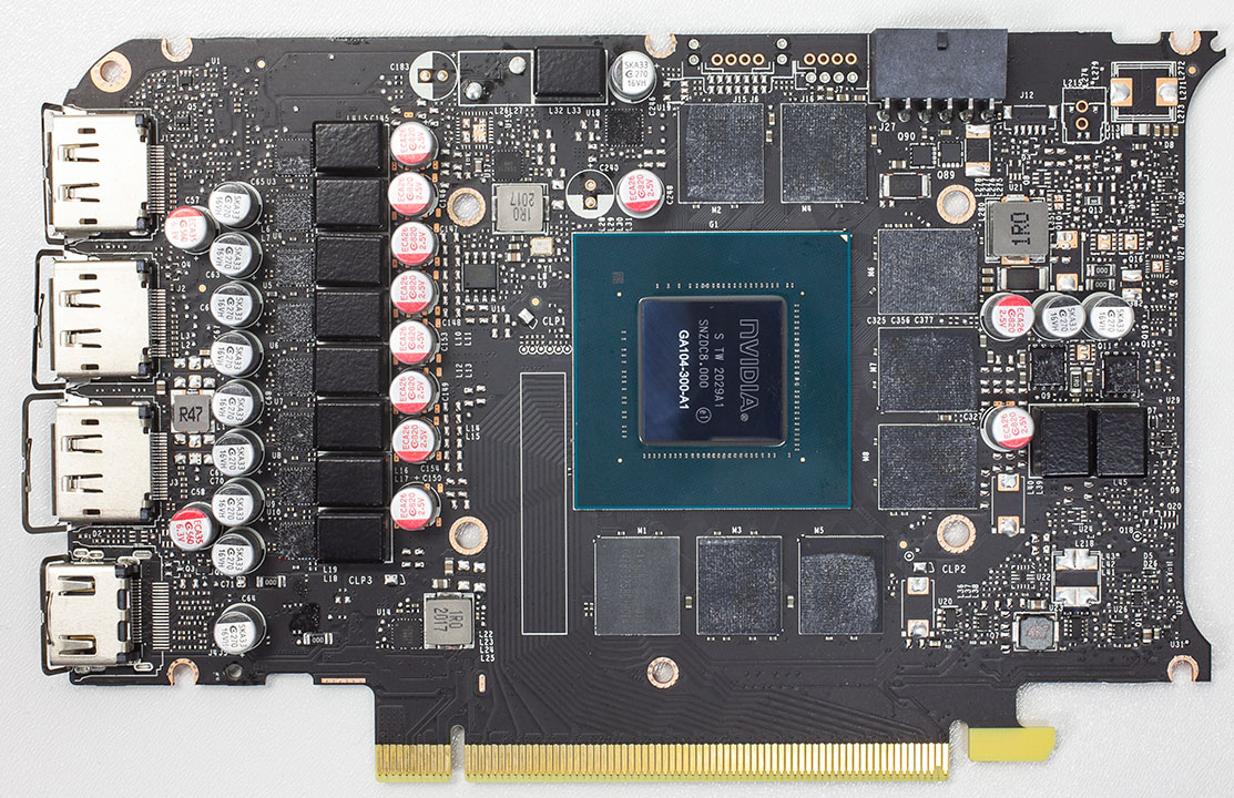

High-res versions are also available (front, back).
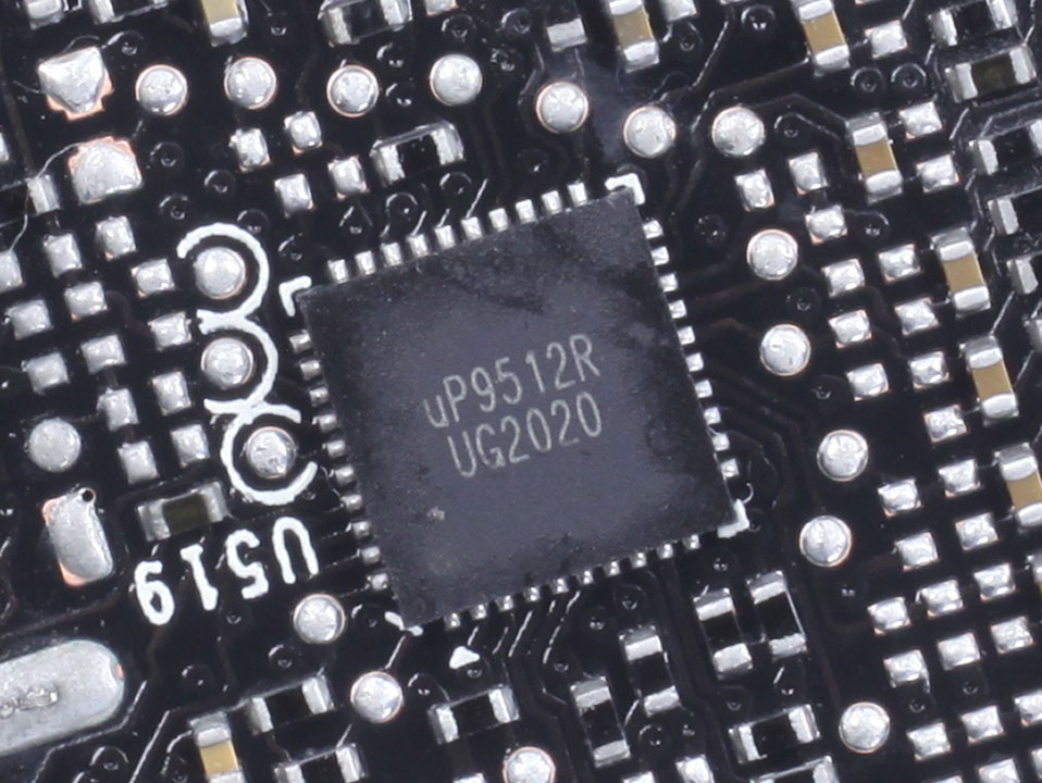
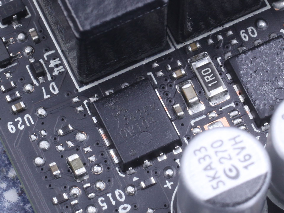
Circuit Board (PCB) Analysis

GPU voltage is 9-phase and managed by a UPI uP9512R controller.

The DrMOS for the GPU are Alpha and Omega AOZ5311.


Memory voltage is a two-phase design generated by a UPI uS5650Q.
For memory, Sinopower SM7342EKKP are used.
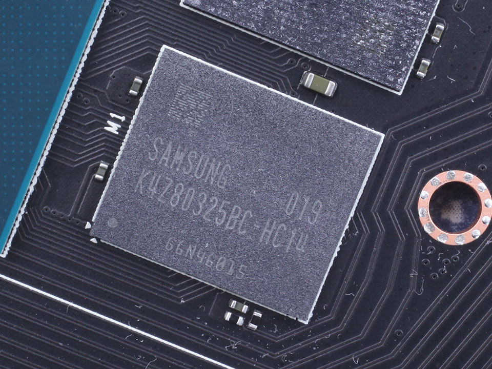
The GDDR6 memory chips are made by Samsung and carry the model number K4Z80325BC-HC14. They are specified to run at 1750 MHz (14 Gbps GDDR6 effective).

NVIDIA's GA104 graphics processor is the company's third Ampere architecture chip, the second one targeted at GeForce gamers. It is produced on a 8 nanometer process at Samsung and has a transistor count of 17.4 billion with a die size of 392 mm².
Apr 15th, 2024 23:28 EDT
change timezone
Latest GPU Drivers
New Forum Posts
- Strange behaviour with my i5 1235u HP laptop after Windows reinstall (2)
- Is it possible that the atmosphere is losing less of its "shield" capabilities due to more and more jets/rockets puncturing it daily? (5)
- FINAL FANTASY XIV: Dawntrail Official Benchmark (27)
- Battery swap for cyberpower UPS (36)
- Dell Workstation Owners Club (3045)
- New pc old gpu intense mouse lag in every aspect (83)
- Your PC ATM (34464)
- Beware: Win11 KB5035853 Cumulative Update may cause stuttering and other performance problems. (12)
- Undervolting Dell XPS 14 9440 is it possible? (2)
- USB C to USB A hub (37)
Popular Reviews
- Horizon Forbidden West Performance Benchmark Review - 30 GPUs Tested
- PowerColor Radeon RX 7900 GRE Hellhound Review
- Galax GeForce RTX 4070 Super EX Review
- Fractal Design Terra Review
- ASUS GeForce RTX 4090 Matrix Platinum Review - The RTX 4090 Ti
- Corsair 2000D Airflow Review
- Minisforum EliteMini UM780 XTX (AMD Ryzen 7 7840HS) Review
- Creative Pebble X Plus Review
- FiiO KB3 HiFi Mechanical Keyboard Review - Integrated DAC/Amp!
- ASUS GeForce RTX 4090 STRIX OC Review
Controversial News Posts
- NVIDIA Points Intel Raptor Lake CPU Users to Get Help from Intel Amid System Instability Issues (102)
- US Government Wants Nuclear Plants to Offload AI Data Center Expansion (98)
- Developers of Outpost Infinity Siege Recommend Underclocking i9-13900K and i9-14900K for Stability on Machines with RTX 4090 (82)
- Sony PlayStation 5 Pro Specifications Confirmed, Console Arrives Before Holidays (80)
- Windows 10 Security Updates to Cost $61 After 2025, $427 by 2028 (79)
- TechPowerUp Hiring: Reviewers Wanted for Motherboards, Laptops, Gaming Handhelds and Prebuilt Desktops (70)
- Intel Realizes the Only Way to Save x86 is to Democratize it, Reopens x86 IP Licensing (70)
- AMD Zen 5 Execution Engine Leaked, Features True 512-bit FPU (63)