 509
509
NVIDIA GeForce RTX 4090 Founders Edition Review - Impressive Performance
Test Setup »High-resolution PCB Pictures
These pictures are for the convenience of volt modders and people who would like to see all the finer details on the PCB. Feel free to link back to us and use these in your articles, videos or forum posts.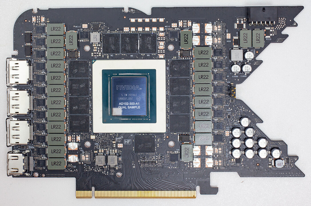
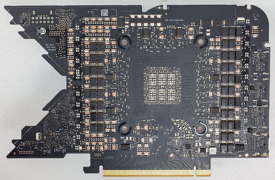
High-resolution versions are also available (front, back).
Circuit Board (PCB) Analysis


GPU voltage is a massive 20-phase design, managed by a Monolithic Power Systems MP2891 controller, which also handles memory voltage.

Monolithic MP86957 DrMOS components are used for GPU voltage; they are rated for 70 A of current each.

Memory voltage is a three-phase design, managed by the same MP2891 that's uses for GPU voltage.

For memory, Monolithic MP86957 DrMOS with a 70 A rating are used again.
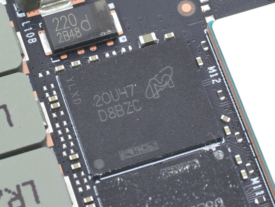
The GDDR6X memory chips are made by Micron and carry the model number D8BZC, which decodes to MT61K512M32KPA-21:U. They are specified to run at 1313 MHz (21 Gbps effective).
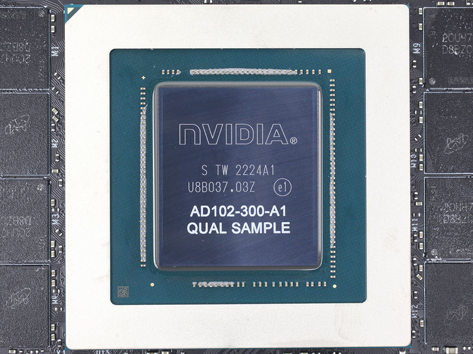
NVIDIA's AD102 graphics processor is the company's flagship Ada Lovelace GPU. It's the world's first 5 nanometer GPU, built at TSMC Taiwan, with a transistor count of 76.3 billion and a die size of 608 mm².
Apr 26th, 2024 03:14 EDT
change timezone
Latest GPU Drivers
New Forum Posts
- Best SSD for system drive (82)
- What phone you use as your daily driver? And, a discussion of them. (1484)
- What's your latest tech purchase? (20342)
- AMD RX 7000 series GPU Owners' Club (1087)
- im new to throttelstop and i think i messed it up by copying others any hints would be very much aprreciated (3)
- Horizontal black lines popping up on my screen? (4)
- Which new games will you be buying? (316)
- Alphacool CORE 1 CPU block - bulging with danger of splitting? (20)
- Black screen after muting (5)
- What are you playing? (20530)
Popular Reviews
- Fractal Design Terra Review
- Thermalright Phantom Spirit 120 EVO Review
- Corsair 2000D Airflow Review
- ASUS GeForce RTX 4090 STRIX OC Review
- NVIDIA GeForce RTX 4090 Founders Edition Review - Impressive Performance
- ASUS GeForce RTX 4090 Matrix Platinum Review - The RTX 4090 Ti
- MSI GeForce RTX 4090 Suprim X Review
- Gigabyte GeForce RTX 4090 Gaming OC Review
- MSI GeForce RTX 4090 Gaming X Trio Review
- MSI GeForce RTX 4090 Suprim Liquid X Review
Controversial News Posts
- Sony PlayStation 5 Pro Specifications Confirmed, Console Arrives Before Holidays (117)
- Windows 11 Now Officially Adware as Microsoft Embeds Ads in the Start Menu (113)
- NVIDIA Points Intel Raptor Lake CPU Users to Get Help from Intel Amid System Instability Issues (106)
- AMD "Strix Halo" Zen 5 Mobile Processor Pictured: Chiplet-based, Uses 256-bit LPDDR5X (101)
- US Government Wants Nuclear Plants to Offload AI Data Center Expansion (98)
- AMD's RDNA 4 GPUs Could Stick with 18 Gbps GDDR6 Memory (88)
- Developers of Outpost Infinity Siege Recommend Underclocking i9-13900K and i9-14900K for Stability on Machines with RTX 4090 (85)
- Windows 10 Security Updates to Cost $61 After 2025, $427 by 2028 (84)