 154
NVIDIA Titan X Pascal 12 GB Review
(154 Comments) »Introduction

A flagship GPU launch by NVIDIA was the last thing we were expecting in the thick of Summer, especially given the market positioning of the GeForce GTX 1080, with some partners running riot with pricing (>$800 prices for some cards) and questionable market availability. NVIDIA managed to surprise us nonetheless by announcing its TITAN X Pascal graphics card barely 10 days ago, with market availability beginning 2nd August, 2016 and our review today.
The most interesting aspect about this brazenly expensive graphics card is its branding. You'll notice that NVIDIA dropped "GeForce GTX" from its model name, simply calling it the "TITAN X Pascal". This makes "TITAN" a consumer graphics brand unto itself. Only NVIDIA's third since GeForce and Riva. This achieves two things. First, it adds to the exclusivity of this SKU, elevating TITAN above GeForce. Second, it adds a bit of ambiguity to whom this product targets as a buyer, letting NVIDIA get away with its steep price tag.
NVIDIA changed tactics to the way it approaches expensive graphics cards with this generation. Earlier, the company would develop a performance-segment chip addressing sub-$600 price-points; and one "big chip" based on the architecture with which it powers high-end GeForce products and Quadro (professional graphics) and Tesla (HPC) products. NVIDIA would find itself with unused on-die components - such as FP64 (double-precision) CUDA cores that made their way to GeForce products - making up a bulk of company's sales for the silicon.
This is something NVIDIA is avoiding with the current generation by developing two "big chips", the GP100, which made its debut with the Tesla P100 HPC accelerator featuring FP64 CUDA cores and exotic HBM2 memory, and the newer GP102 silicon, which is designed keeping in mind consumer graphics and professional graphics applications that don't use double-precision compute. This chip also trades HBM2 for the more affordable GDDR5X memory.
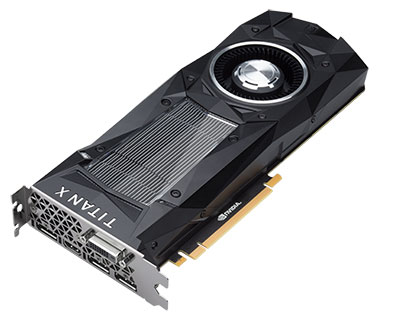
The reviewed TITAN X Pascal is the first product based on the GP102 silicon. It physically features 3,840 CUDA cores spread across 30 streaming multiprocessors (SM) and six graphics processing clusters (GPCs) from which 3,584 are enabled on the TITAN X Pascal. The GP102 is in essence a 1.5X upscale of the GP104 silicon. Also featured are 224 TMUs, 96 ROPs, and a 384-bit wide GDDR5X memory interface holding 12 GB of memory.
Due to lack of any real competition from AMD in the current generation, NVIDIA gets to be cocky with its pricing. NVIDIA is pricing the TITAN X Pascal at a staggering $1,200. The company is directly marketing the card, doing away with add-in card (AIC) partners (eg: ASUS, EVGA, Zotac, etc.). The company is also supplying the card through the OEM channel, to pre-built gaming PC vendors (eg: CyberPowerPC, Alienware, etc.).
| Radeon R9 Fury X | GeForce GTX 980 Ti | GeForce GTX Titan X | GeForce GTX 1070 | GeForce GTX 1080 | Titan X Pascal | |
|---|---|---|---|---|---|---|
| Shader Units | 4096 | 2816 | 3072 | 1920 | 2560 | 3584 |
| ROPs | 64 | 96 | 96 | 64 | 64 | 96 |
| Graphics Processor | Fiji | GM200 | GM200 | GP104 | GP104 | GP102 |
| Transistors | 8900M | 8000M | 8000M | 7200M | 7200M | 12000M |
| Memory Size | 4 GB | 6 GB | 12 GB | 8 GB | 8 GB | 12 GB |
| Memory Bus Width | 4096 bit | 384 bit | 384 bit | 256 bit | 256 bit | 384 bit |
| Core Clock | 1050 MHz | 1000 MHz+ | 1000 MHz+ | 1506 MHz+ | 1607 MHz+ | 1418 MHz+ |
| Memory Clock | 500 MHz | 1750 MHz | 1750 MHz | 2002 MHz | 1251 MHz | 1251 MHz |
| Price | $600 | $440 | $1150 | $380 / $450 | $600 / $700 | $1200 |
Architecture
The TITAN X Pascal is based on NVIDIA's new second-biggest chip based on the "Pascal" architecture, the GP102 silicon. The biggest GPU is the GP100 driving the Tesla P100 HPC processor. The GP102 is essentially GP100 minus FP64 CUDA cores, featuring only 3,840 FP32 ones, and 4096-bit HBM2 memory interface making way for 384-bit GDDR5X. As mentioned earlier, the GP102 is a 1.5X upscale of the GP104 silicon, which powers the GeForce GTX 1080.


With each successive architecture since "Fermi," NVIDIA has been enriching the streaming multiprocessor (SM) by adding more dedicated resources and reducing shared resources within the graphics processing cluster (GPC), which leads to big performance gains. The story continues with "Pascal." Like the GM200 before it, the GP102 features six GPCs, super-specialized subunits of the GPU that share the PCI-Express 3.0 x16 host interface and the 384-bit GDDR5X memory interface through twelve controllers. These controllers support GDDR5X memory, ticking at 10 Gbps.
Workload across the six GPCs is shared by the GigaThread Engine cushioned by 3 MB of cache. Each GPC holds five streaming multiprocessors (SMs), which is an increase from the four SMs each GPC held on the GM200. The GPC shares a raster engine between these five SMs. The "Pascal" streaming multiprocessor features a 4th generation PolyMorph Engine, a component for key render setup operations. With "Pascal," the PolyMorph Engine includes specialized hardware for the new Simultaneous MultiProjection feature. Each SM also holds a block of eight TMUs.
Each SM continues to feature 128 CUDA cores. The GP102 hence features a total of 3,840 CUDA cores, from which 3,584 across 28 SMs are enabled on the TITAN X Pascal. Other vital specifications include 224 TMUs and 96 ROPs. NVIDIA claims to have worked on a new GPU internal circuit design and board channel paths to facilitate significantly higher clock speeds than what the GM204 is capable of. The TITAN X Pascal ships with 1417 MHz GPU clock speed, and a maximum GPU Boost frequency of 1531 MHz. These look like lower clock speeds than what the GTX 1080 ships with, but one has to understand that the GP102 is a much bigger chip, and even with the current speeds, its TDP is rated at 250W. For comparison, the original GeForce GTX TITAN X (Maxwell) was clocked at 1000 MHz, with 1089 MHz boost.

The TITAN X Pascal features the new GDDR5X memory standard. The interface enables effective data-rates that are as high as 14 GHz, and although it has many bare-metal specifications in common with GDDR5, minimizing R&D for its implementation, the memory chip design is improved with higher pin counts to support these higher data-rates. The memory is clocked at an effective 10 GHz. Over a 384-bit memory interface, this works out to a memory bandwidth of 480 GB/s NVIDIA has also optimized the usage of with more advanced 4th generation lossless Delta Color Compression. The best-case scenario has Delta Color Compression provide an "effective" memory bandwidth uplift of 20 percent, which results in 576 GB/s.

The "Pascal" architecture supports Asynchronous Compute as standardized by Microsoft. It adds to that with its own variation of the concept with "Dynamic Load Balancing."


Packaging


You will receive:
- Graphics card
- Documentation
The Card
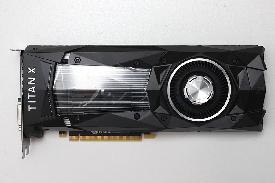
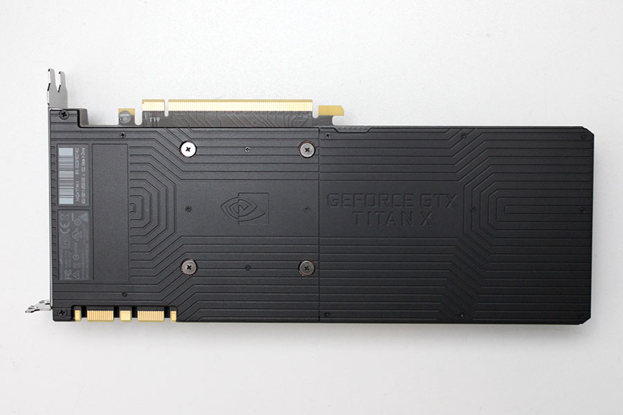
NVIDIA's Titan X Pascal cooler design is identical to that of the GeForce GTX 1080 Founders Edition. The only change is that the cooler is black instead of silver. NVIDIA even kept the illuminated "GeForce GTX" logo on the side. On the back, you will find the same backplate as on the GTX 1080, which can be partially removed to improve airflow for SLI. Dimensions of the card are 27 cm x 11 cm.

Installation requires two slots in your system.

Display connectivity options include a DVI port, an HDMI port, and three DisplayPorts. Unlike previous NVIDIA cards, the DVI port no longer includes the analog signal, so you'll have to use an active adapter. NVIDIA also updated DisplayPort to be 1.2 certified and 1.3/1.4 ready, which enables support for 4K at 120 Hz and 5K @ 60 Hz, or 8K @ 60 Hz with two cables.
The GPU also comes with an HDMI sound device. It is HDMI 2.0b compatible, which supports HD audio and Blu-ray 3D movies. The GPU video encoding unit has been updated to support HEVC at 10-bit and 12-bit.

With Pascal, NVIDIA made some changes to how SLI works. In a nutshell, for 4K at 60 Hz and above, NVIDIA recommends new high-bandwidth SLI bridges it dubbed "SLI HB." These bridges occupy both SLI fingers. Traditional triple- and quad-SLI setups are gone as well. Only certain benchmarks can run more than the dual-SLI setup to which all games are limited.
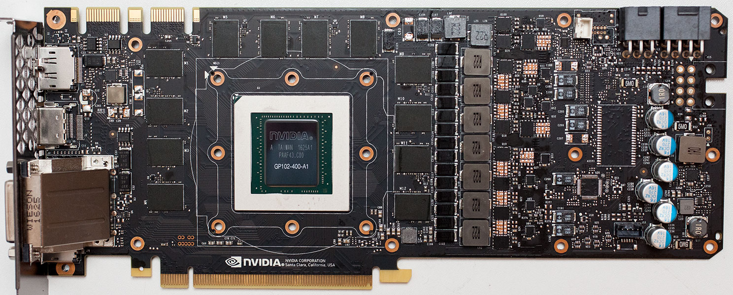

Pictured above are the front and back, showing the disassembled board. High-res versions are also available (front, back).
Our Patreon Silver Supporters can read articles in single-page format.
Nov 11th, 2026 20:27 CST
change timezone
New Forum Posts
- Classic Blizzard games (WarCraft 1-2, Diablo 1-2, StarCraft 1) (3)
- TPU's Nostalgic Hardware Club (22144)
- When you could finally run Crysis maxed out? (45)
- Your PC ATM (36401)
- Gacha Games - Discussions, Pulls, Updates, etc. (1149)
- Steam Deck Owners Clubhouse (618)
- Ryzen 7 8700G OC (0)
- Case to fit 2X Alphacool NexXxoS UT60 Rads (5)
- AAF Optimus Modded Driver For Windows 10 & 11 - Only for HDAUDIO Chips [WINDOWS 11 RECOMMENDED] (1153)
- Samsung 870 EVO - Beware, certain batches prone to failure! (1487)
Popular Reviews
- AMD Zen 6 Technical Deep Dive
- Upcoming Hardware Launches 2027 (Updated Nov 2026)
- XPG NIMBUS PLUS Review - Mid-range Chair With Strong Competitors
- NZXT H7 RGB+ Review
- NZXT H5 Review
- NZXT C1200 Platinum Review
- Phantom Blade Zero Performance Benchmark Review - 35 GPUs Tested
- Montech King 95 3D PRO Review
- Gigabyte Z890I Aorus Ultra Review
- INNOCN 45C1R Review - Two QHD Screens, Zero Bezels
TPU on YouTube
Controversial News Posts
- OpenAI CEO Argues Home PCs Waste the World's Limited DRAM Supply (152)
- NVIDIA Launches Investigation Into Jensen Huang's Relationship With Suspected Chinese Spy (136)
- Intel "Raptor Lake Next" 16-Core and 20-Core CPUs Surface (130)
- Legendary Game Studio BioWare Shuts Down Following EA Layoffs (104)
- Dell CEO Says the Memory Shortage Will Get Worse in 2027 (95)
- NVIDIA GeForce RTX 50-Series Scheduled for up to $500 Price Hike This Week (89)
- AMD Radeon Owners Can Now Run Nearly Every DLSS Feature Through Fan-Made Mod (80)
- Modder Fits RTX 5090 With Four 8-Pin Connectors, Halving Current per Wire (80)