 27
27
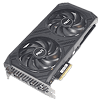
Palit GeForce RTX 4060 Dual Review
Test Setup »High-resolution PCB Pictures
These pictures are for the convenience of volt modders and people who would like to see all the finer details on the PCB. Feel free to link back to us and use these in your articles, videos or forum posts.

High-resolution versions are also available (front, back).
Circuit Board (PCB) Analysis


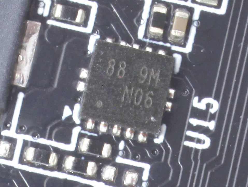
GPU voltage is handled by a 4-phase VRM driven by a Richtek RT8845A controller

Sinopower 4507NH and 4503NH discrete MOSFETs are used for the GPU phases, these are rated for 60 A.

Memory voltage is a single-phase design, and handled by a buck controller.

For memory, the Sinopower 4507NH and 4503NH discrete MOSFET combo make a comeback, rated for 60 A.
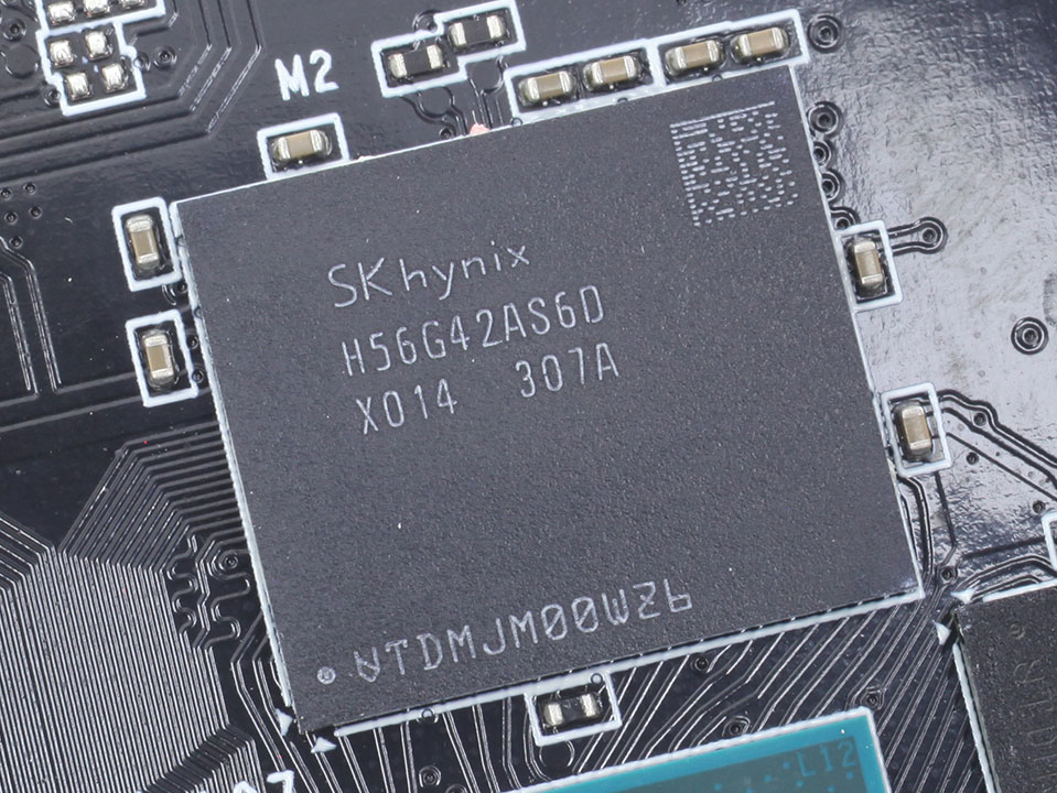
The GDDR6 memory chips are made by Hynix and carry the model number H56G42AS6DX-014. They are specified to run at 2250 MHz (18 Gbps effective).

NVIDIA's AD107 graphics processor is the company's smallest Ada Lovelace GPU. It is built using a 5 nanometer process at TSMC Taiwan, with a transistor count of 18.9 billion and a die size of 156 mm².
May 10th, 2024 12:12 EDT
change timezone
Latest GPU Drivers
New Forum Posts
- Battery swap for cyberpower UPS (75)
- looking to optimize (performance+cooling) a ryzen 7800x3d system with x670e aorus pro x (19)
- Homeworld 3 [Official Thread] (10)
- Keysfan (27)
- EKWB - ideas for IMPROVING products and NEW products (5)
- Intel SSD model codes & SanDisk SSD product codes reference list (1)
- What's your latest tech purchase? (20501)
- Issues with my gaming laptop (2)
- What's a good option for a digital touchless thermometer? (20)
- What are you playing? (20613)
Popular Reviews
- CHERRY XTRFY M64 Pro Review
- Bykski CPU-XPR-C-I CPU Water Block Review - Amazing Value!
- Corsair iCUE Link RX120 RGB 120 mm Fan Review
- ThundeRobot ML903 NearLink Review
- Corsair MP700 Pro SE 4 TB Review
- Upcoming Hardware Launches 2023 (Updated Feb 2024)
- Finalmouse UltralightX Review
- AMD Ryzen 7 7800X3D Review - The Best Gaming CPU
- Sapphire Radeon RX 7700 XT Pure Review
- ZMF Caldera Closed Planar Magnetic Headphones Review
Controversial News Posts
- Intel Statement on Stability Issues: "Motherboard Makers to Blame" (264)
- AMD to Redesign Ray Tracing Hardware on RDNA 4 (206)
- Windows 11 Now Officially Adware as Microsoft Embeds Ads in the Start Menu (170)
- NVIDIA to Only Launch the Flagship GeForce RTX 5090 in 2024, Rest of the Series in 2025 (144)
- Sony PlayStation 5 Pro Specifications Confirmed, Console Arrives Before Holidays (119)
- AMD's RDNA 4 GPUs Could Stick with 18 Gbps GDDR6 Memory (114)
- NVIDIA Points Intel Raptor Lake CPU Users to Get Help from Intel Amid System Instability Issues (106)
- AMD Ryzen 9 7900X3D Now at a Mouth-watering $329 (104)