 1
1
Palit GeForce RTX 4060 Ti Dual OC Review
(1 Comment) »Introduction
Palit GeForce RTX 4060 Ti Dual OC is the company's affordable yet factory-overclocked custom-design rendition of NVIDIA's latest performance segment graphics card. The Dual series of graphics cards form Palit's most affordable product offerings in any series, and the RTX 4060 Ti Dual OC in this review has a sibling that sticks to NVIDIA-reference clock speeds, although we're not sure if it also sells at the $399 MSRP. The Dual OC is priced at a "small premium," Palit didn't give us any exact number. If you're wondering why you're seeing many custom-design RTX 4060 Ti reviews being published today (May 24), it's because NVIDIA gave the cards that sell at its MSRP a 1-day advantage with the review postings.
The new NVIDIA GeForce RTX 4060 Ti is designed to help NVIDIA consolidate in the crucial performance segment, with its starting price of $399 that's unchanged from that of the RTX 3060 Ti. It is designed for 1080p AAA gaming with nearly maxed-out settings, including ray tracing, while also being capable of 1440p if you know your way around game settings, or can get GeForce Experience to find the right ones for you. The GeForce RTX 4060 Ti is among a 3-part RTX 4060 series NVIDIA is planning for at three distinct price points. The RTX 4060 Ti launching today has a $399 MSRP, and comes with an 8 GB VRAM size. Its 16 GB variant bound for July is priced at $500, and the most affordable RTX 4060 at $299. All three have essentially the same use-case of 1080p gaming at varying grades of eye-candy.

The GeForce RTX 4060 Ti is very much a next-generation graphics card, it's based on the Ada Lovelace graphics architecture, and 5 nm silicon, so you get generational performance/watt uplifts, besides a few exclusive features such as DLSS 3 Frame Generation—a feature that leverages the Optical Flow Accelerator component to draw entire frames purely out of AI, without involving the graphics rendering pipeline. This effectively doubles frame-rates in games that are optimized for the feature. DLSS 3 is of particular significance in this market-segment, where the framerate doubling can be used to dial up settings, or even display resolution. The Ada Lovelace graphics architecture debuts the 3rd generation of RTX, NVIDIA's ground-breaking technology that combines real time ray traced elements with conventional raster 3D graphics. NVIDIA has made its RT cores—now in their third generation—more capable and independent of the general purpose CUDA cores; and made its AI-accelerating Tensor cores (4th Gen) more capable, with support for newer math formats.
The RTX 4060 Ti is based on the 5 nm AD106 silicon, which it nearly maxes out, by featuring 34 out of 36 streaming multiprocessors (SM) physically present. This translates to 4,352 CUDA cores, 136 Tensor cores, 34 RT cores, 136 TMUs, and 48 ROPs. The card gets the same 8 GB of memory size as the RTX 3060 Ti, but a narrower 128-bit memory interface. NVIDIA is using faster 18 Gbps memory chips, but the real innovation, the company claims, is at an architectural-level, with greater emphasis on large on-die caches that reduce the roundtrips to the video memory, allowing NVIDIA to slim down the memory interface to undoubtedly save costs.
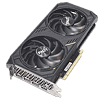
The Palit RTX 4060 Ti Dual OC is a simple affair, with a lightweight, dual-slot, aluminium fin-stack heatsink that's ventilated by a pair of fans (which is where the SKU gets its name from). The card offers factory-overclocked speeds of 2685 MHz boost, compared to 2535 MHz reference boost; while the memory is left untouched at 18 Gbps. Palit opted for a single 8-pin PCIe power connector instead of the fancy new 16-pin ATX 12VHPWR, which should help a great deal with compatibility. With a TGP of just 160 W, there's plenty of power on tap, even for a factory-overclocked card. Palit hasn't provided us with any pricing, only "slightly above MSRP," so we'll be using $420 throughout this review.
| Price | Cores | ROPs | Core Clock | Boost Clock | Memory Clock | GPU | Transistors | Memory | |
|---|---|---|---|---|---|---|---|---|---|
| RTX 2060 | $180 | 1920 | 48 | 1365 MHz | 1680 MHz | 1750 MHz | TU106 | 10800M | 6 GB, GDDR6, 192-bit |
| RX Vega 64 | $320 | 4096 | 64 | 1247 MHz | 1546 MHz | 953 MHz | Vega 10 | 12500M | 8 GB, HBM2, 2048-bit |
| RX 5700 XT | $180 | 2560 | 64 | 1605 MHz | 1755 MHz | 1750 MHz | Navi 10 | 10300M | 8 GB, GDDR6, 256-bit |
| RTX 3050 | $260 | 2560 | 32 | 1552 MHz | 1777 MHz | 1750 MHz | GA106 | 12000M | 8 GB, GDDR6, 128-bit |
| RTX 2070 | $230 | 2304 | 64 | 1410 MHz | 1620 MHz | 1750 MHz | TU106 | 10800M | 8 GB, GDDR6, 256-bit |
| RX 6600 | $210 | 1792 | 64 | 2044 MHz | 2491 MHz | 1750 MHz | Navi 23 | 11060M | 8 GB, GDDR6, 128-bit |
| RTX 3060 | $300 | 3584 | 48 | 1320 MHz | 1777 MHz | 1875 MHz | GA106 | 12000M | 12 GB, GDDR6, 192-bit |
| RTX 4060 | $300 | 3072 | 32 | 1830 MHz | 2460 MHz | 2125 MHz | AD107 | unknown | 8 GB, GDDR6, 128-bit |
| RX 6600 XT | $250 | 2048 | 64 | 2359 MHz | 2589 MHz | 2000 MHz | Navi 23 | 11060M | 8 GB, GDDR6, 128-bit |
| Arc A750 | $250 | 3584 | 112 | 2050 MHz | N/A | 2000 MHz | ACM-G10 | 21700M | 8 GB, GDDR6, 256-bit |
| Arc A770 | $290 | 4096 | 128 | 2100 MHz | N/A | 2187 MHz | ACM-G10 | 21700M | 16 GB, GDDR6, 256-bit |
| RTX 2080 | $260 | 2944 | 64 | 1515 MHz | 1710 MHz | 1750 MHz | TU104 | 13600M | 8 GB, GDDR6, 256-bit |
| RTX 3060 Ti | $320 | 4864 | 80 | 1410 MHz | 1665 MHz | 1750 MHz | GA104 | 17400M | 8 GB, GDDR6, 256-bit |
| RTX 4060 Ti | $400 | 4352 | 48 | 2310 MHz | 2535 MHz | 2250 MHz | AD106 | 22900M | 8 GB, GDDR6, 128-bit |
| Palit RTX 4060 Ti Dual OC | $420 | 4352 | 48 | 2310 MHz | 2685 MHz | 2250 MHz | AD106 | 22900M | 8 GB, GDDR6, 128-bit |
| RX 6700 XT | $320 | 2560 | 64 | 2424 MHz | 2581 MHz | 2000 MHz | Navi 22 | 17200M | 12 GB, GDDR6, 192-bit |
| RTX 2080 Ti | $400 | 4352 | 88 | 1350 MHz | 1545 MHz | 1750 MHz | TU102 | 18600M | 11 GB, GDDR6, 352-bit |
| RTX 3070 | $350 | 5888 | 96 | 1500 MHz | 1725 MHz | 1750 MHz | GA104 | 17400M | 8 GB, GDDR6, 256-bit |
| RTX 3070 Ti | $420 | 6144 | 96 | 1575 MHz | 1770 MHz | 1188 MHz | GA104 | 17400M | 8 GB, GDDR6X, 256-bit |
Architecture
The Ada graphics architecture heralds the third generation of the NVIDIA RTX technology, an effort toward increasing the realism of game visuals by leveraging real-time ray tracing, without the enormous amount of compute power required to draw purely ray-traced 3D graphics. This is done by blending conventional raster graphics with ray traced elements such as reflections, lighting, and global illumination, to name a few. The 3rd generation of RTX introduces the new higher IPC "Ada" CUDA core, 3rd generation RT core, 4th generation Tensor core, and the new Optical Flow Processor, a component that plays a key role in generating new frames without involving the GPU's main graphics rendering pipeline.


The GeForce Ada graphics architecture driving the RTX 4060 Ti leverages the TSMC 5 nm EUV foundry process to increase transistor counts. At the heart of this GPU is the new AD106 silicon, with a fairly high transistor count of 22.9 billion, which is almost double that of the previous-generation GA106, and still about 30% more than the GA104. The GPU features a generationally narrower PCI-Express 4.0 x8 host interface, and a 128-bit wide GDDR6 memory interface. This is causing some controversy, and we'll present NVIDIA's explanation below. The Optical Flow Accelerator (OFA) is an independent top-level component. The chip features one NVENC and one NVDEC unit.
The essential component hierarchy is similar to past generations of NVIDIA GPUs. The AD106 silicon features 3 Graphics Processing Clusters (GPCs), each of these has all the SIMD and graphics rendering machinery, and is a small GPU in its own right. Each GPC shares a raster engine (geometry processing components) and two ROP partitions (each with eight ROP units). The GPC of the AD106 contains five Texture Processing Clusters (TPCs), the main number-crunching machinery. Each of these has two Streaming Multiprocessors (SM), and a Polymorph unit. Each SM contains 128 CUDA cores across four partitions. Half of these CUDA cores are pure-FP32; while the other half is capable of FP32 or INT32. The SM retains concurrent FP32+INT32 math processing capability. The SM also contains a 3rd generation RT core, four 4th generation Tensor cores, some cache memory, and four TMUs. There are 12 SM per GPC, so 1,536 CUDA cores, 48 Tensor cores, and 12 RT cores; per GPC. There are three such GPCs, which add up to 4,608 CUDA cores, 144 TMUs, 144 Tensor Cores, and 36 RT cores. Each GPC contributes 16 ROPs, so there are 48 ROPs on the silicon. The RTX 4060 Ti is carved out of the AD106 by disabling one TPC worth 256 CUDA cores. This yields 4,352 CUDA cores, 136 Tensor cores, 34 RT cores, and 136 TMUs. The ROP count is untouched at 48, as is the on-die L2 cache sees a slight reduction, which is 32 MB in size.


The 3rd generation RT core accelerates the most math-intensive aspects of real-time ray tracing, including BVH traversal. Displaced micro-mesh engine is a revolutionary feature introduced with the new 3rd generation RT core. Just as mesh shaders and tessellation have had a profound impact on improving performance with complex raster geometry, allowing game developers to significantly increase geometric complexity; DMMs is a method to reduce the complexity of the bounding-volume hierarchy (BVH) data-structure, which is used to determine where a ray hits geometry. Previously, the BVH had to capture even the smallest details to properly determine the intersection point. Ada's ray tracing architecture also receives a major performance uplift from Shader Execution Reordering (SER), a software-defined feature that requires awareness from game-engines, to help the GPU reorganize and optimize worker threads associated with ray tracing.


The BVH now needn't have data for every single triangle on an object, but can represent objects with complex geometry as a coarse mesh of base triangles, which greatly simplifies the BVH data structure. A simpler BVH means less memory consumed and helps to greatly reduce ray tracing CPU load, because the CPU only has to generate a smaller structure. With older "Ampere" and "Turing" RT cores, each triangle on an object had to be sampled at high overhead, so the RT core could precisely calculate ray intersection for each triangle. With Ada, the simpler BVH, plus the displacement maps can be sent to the RT core, which is now able to figure out the exact hit point on its own. NVIDIA has seen 11:1 to 28:1 compression in total triangle counts. This reduces BVH compile times by 7.6x to over 15x, in comparison to the older RT core; and reducing its storage footprint by anywhere between 6.5 to 20 times. DMMs could reduce disk- and memory bandwidth utilization, utilization of the PCIe bus, as well as reduce CPU utilization. NVIDIA worked with Simplygon and Adobe to add DMM support for their tool chains.


Opacity Micro Meshes (OMM) is a new feature introduced with Ada to improve rasterization performance, particularly with objects that have alpha (transparency data). Most low-priority objects in a 3D scene, such as leaves on a tree, are essentially rectangles with textures on the leaves where the transparency (alpha) creates the shape of the leaf. RT cores have a hard time intersecting rays with such objects, because they're not really in the shape that they appear (they're really just rectangles with textures that give you the illusion of shape). Previous-generation RT cores had to have multiple interactions with the rendering stage to figure out the shape of a transparent object, because they couldn't test for alpha by themselves.


This has been solved by using OMMs. Just as DMMs simplify geometry by creating meshes of micro-triangles; OMMs create meshes of rectangular textures that align with parts of the texture that aren't alpha, so the RT core has a better understanding of the geometry of the object, and can correctly calculate ray intersections. This has a significant performance impact on shading performance in non-RT applications, too. Practical applications of OMMs aren't just low-priority objects such as vegetation, but also smoke-sprites and localized fog. Traditionally there was a lot of overdraw for such effects, because they layered multiple textures on top of each other, that all had to be fully processed by the shaders. Now only the non-opaque pixels get executed—OMMs provide a 30 percent speedup with graphics buffer fill-rates, and a 10 percent impact on frame-rates.


DLSS 3 introduces a revolutionary new feature that promises a doubling in frame-rate at comparable quality, it's called AI frame-generation. While it has all the features of DLSS 2 and its AI super-resolution (scaling up a lower-resolution frame to native resolution with minimal quality loss); DLSS 3 can generate entire frames simply using AI, without involving the graphics rendering pipeline. Later in the article, we will show you DLSS 3 in action.


Every alternating frame with DLSS 3 is hence AI-generated, without being a replica of the previous rendered frame. This is possible only on the Ada graphics architecture, because of a hardware component called the optical flow accelerator (OFA), which assists in predicting what the next frame could look like, by creating what NVIDIA calls an optical flow-field. OFA ensures that the DLSS 3 algorithm isn't confused by static objects in a rapidly-changing 3D scene (such as a race sim). The process heavily relies on the performance uplift introduced by the FP8 math format of the 4th generation Tensor core. A third key ingredient of DLSS 3 is Reflex. By reducing the rendering queue to zero, Reflex plays a vital role in ensuring that frame-times with DLSS 3 are at an acceptable level, and a render-queue doesn't confuse the upscaler. A combination of OFA and the 4th Gen Tensor core is why the Ada architecture is required to use DLSS 3, and why it won't work on older architectures.
Ada Rebalanced Memory Subsystem


The previous-generation GeForce RTX 3060 Ti featured a 256-bit wide GDDR6 memory interface driving its 8 GB of 14 Gbps-rated GDDR6 memory (448 GB/s memory bandwidth), which has caused some controversy with the new RTX 4060 Ti using a narrower 128-bit wide memory interface to drive 8 GB of 18 Gbps memory (288 GB/s bandwidth). With the new Ada Lovelace graphics architecture, NVIDIA has tried to re-balance the memory sub-system such that there's dependence on larger on-die caches, allowing NVIDIA to narrow down the GPU's GDDR6 memory interface. The obvious benefit of this to NVIDIA is reduced costs, let's make no mistake about it, but NVIDIA maintains that this isn't a big problem for the GPU.
The last-level cache, or L2 cache, of NVIDIA Ada GPUs is anywhere between 8-10 times larger than the ones on the previous-generation Ampere GPUs. The AD106 silicon powering the RTX 4060 Ti has a 32 MB L2 cache, compared to the 4 MB of the GA104 silicon powering the RTX 3060 Ti. NVIDIA illustrated an example of how the larger on-die LLC reduces video memory pressure (trips to GDDR6) by anywhere between 40% to 60% on the same GPU, by soaking up a larger number of memory access requests by the shaders.
The L2 cache is unified victim cache to the GPU's various GPCs and their local TPCs. Data that isn't hot enough (frequently accessed enough) to be resident on the small L1 caches of the SM, is ejected to the L2 cache, and depending on its heat, pushed to the GDDR6 video memory. The L2 cache is an order of magnitude faster than than video memory in terms of latency, so having frequently-accessed data reside there offers a considerable benefit.

As we mentioned earlier from NVIDIA's claims, this re-balancing of the memory sub-system between the on-die LLC and video memory lowers the GPU's access to the latter by as much as 60%, which means the GPU can make do with a narrower 128-bit wide GDDR6 memory bus. NVIDIA has used generationally faster 18 Gbps memory chips in the RTX 4060 Ti. NVIDIA developed a new means of presenting the memory bandwidth that takes into account the contribution of the L2 cache, its hit-rate, and the consequent reduction in video memory traffic. While the memory bandwidth of the RTX 4060 Ti is 288 GB/s, NVIDIA claims that its "effective bandwidth" is 554 GB/s (23% higher than the 448 GB/s memory bandwidth of the RTX 3060 Ti). It's interesting to point out that NVIDIA has used "effective bandwidth" figures in the past to highlight its lossless memory compression technologies, but has never been this vocal about it.
Packaging
The Card
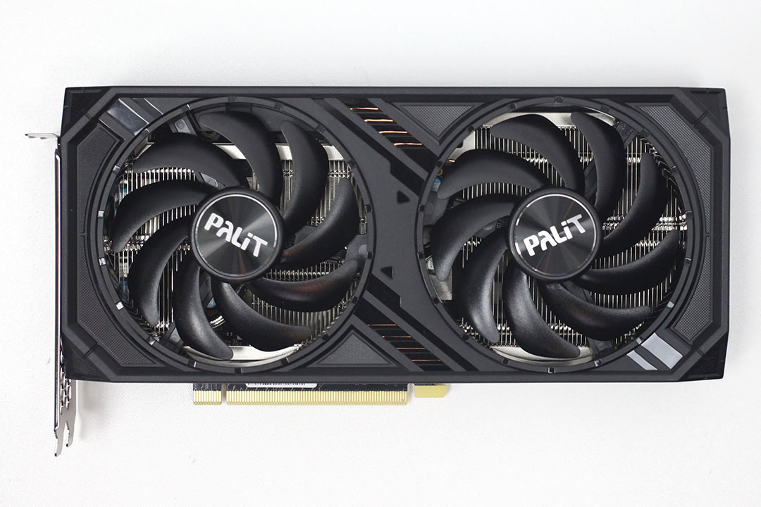

Palit RTX 4060 Ti Dual OC has a very conventional-looking design that looks like it can be sold very close to the NVIDIA MSRP. The sporty-looking cooler shroud, as well as the backplate, are made of plastic.

Palit has placed an RGB illuminated zone near the top right of the card.


Dimensions of the card are 25.0 x 12.0 cm, and it weighs 621 g.


Installation requires two slots in your system.

Display connectivity includes three standard DisplayPort 1.4a ports and one HDMI 2.1a (same as Ampere).
The new 8th Gen NVENC now accelerates AV1 encoding, besides HEVC. You also get an "optical flow accelerator" unit that is able to calculate intermediate frames for videos, to smooth playback. The same hardware unit is used for frame generation in DLSS 3.

The card uses a single classic 8-pin PCIe power connector, which should be more convenient and easier to deal with than the 12VHPWR connector used on the FE model.
Teardown

Disassembling the Palit Dual OC is pretty straightforward. You undo a series of screws, first the backplate comes off, then the heatsink follows.

The Palit Dual OC cooler design is a simple fare, a copper base-plate makes contact with the GPU, surrounded by an aluminium one, which pulls heat from the memory chips. The baseplate region has its own set of aluminium fins. Three nickel-plated copper heatpipes pass through, with two additional fin-stacks at their ends.

The card uses three nickel-plated copper heat pipes to spread heat across the cooler.


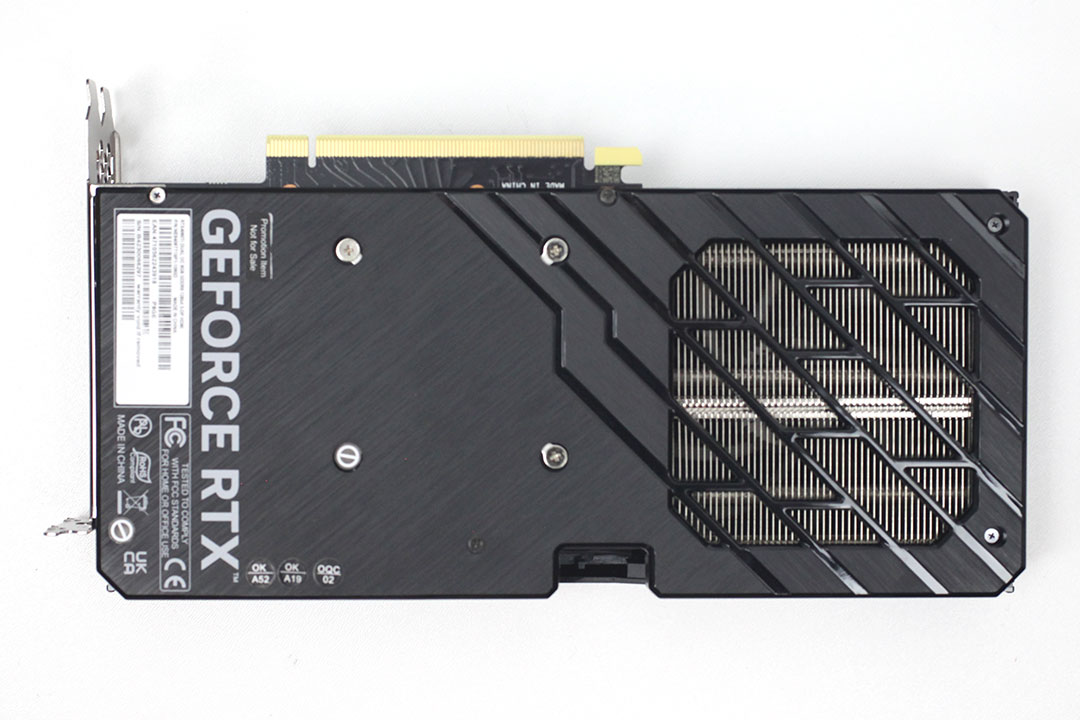
The backplate is made of plastic. We like how Palit it put in effort to give it a brushed aluminium appearance.
High-resolution PCB Pictures
These pictures are for the convenience of volt modders and people who would like to see all the finer details on the PCB. Feel free to link back to us and use these in your articles, videos or forum posts.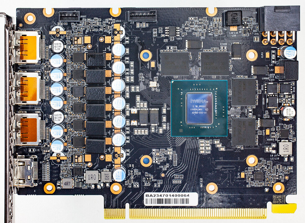

High-resolution versions are also available (front, back).
Our Patreon Silver Supporters can read articles in single-page format.
Jun 2nd, 2024 05:22 EDT
change timezone
Latest GPU Drivers
New Forum Posts
- Anyone born in the 70s? Remember how good the 90s games were? (15)
- 3DMARK "LEGENDARY" (214)
- Core counting (68)
- How to reduce Asus mining rx470 4096 mb to 2048 mb vram? (8)
- Z890/X870 feature dreamlist (31)
- Dude, youre hotrodding a Dell... (4)
- can a damaged motherboard onboard audio cause randomly audio popping / crackling? (20)
- How do you get games for PC? (17)
- What's your latest tech purchase? (20718)
- Flash original BIOS - Asrock RX570 (1)
Popular Reviews
- SilverStone KL07E Review
- ID-Cooling FX360 PRO Review - Shots Fired @ Arctic
- NuPhy Air96 V2 Low Profile Wireless Mechanical Keyboard Review
- Upcoming Hardware Launches 2024 (Updated May 2024)
- Montech Titan Gold 1000 W Review
- Elysian Acoustic Labs Pilgrim In-Ear Monitors Review
- Senua’s Saga: Hellblade II: DLSS vs. FSR vs. XeSS Comparison Review
- Ghost of Tsushima Performance Benchmark Review - 35 GPUs Tested
- Senua's Saga: Hellblade II Performance Benchmark Review
- AMD Ryzen 7 7800X3D Review - The Best Gaming CPU
Controversial News Posts
- AMD to Redesign Ray Tracing Hardware on RDNA 4 (227)
- NVIDIA to Only Launch the Flagship GeForce RTX 5090 in 2024, Rest of the Series in 2025 (154)
- AMD Hits Highest-Ever x86 CPU Market Share in Q1 2024 Across Desktop and Server (140)
- AMD RDNA 5 a "Clean Sheet" Graphics Architecture, RDNA 4 Merely Corrects a Bug Over RDNA 3 (139)
- NVIDIA RTX 5090 "Blackwell" Founders Edition to Implement the "RTX 4090 Ti" Cinderblock Design (118)
- Core Configurations of Intel Core Ultra 200 "Arrow Lake-S" Desktop Processors Surface (101)
- Biden Administration to Revive Trump-Era Tariffs on China-made GPUs and Motherboards (95)
- AMD Ryzen 9000 Zen 5 Single Thread Performance at 5.80 GHz Found 19% Over Zen 4 (88)