 6
6
Palit GeForce RTX 4070 Ti Super Jetstream OC Review
Test Setup »High-resolution PCB Pictures
These pictures are for the convenience of volt modders and people who would like to see all the finer details on the PCB. Feel free to link back to us and use these in your articles, videos or forum posts.

High-resolution versions are also available (front, back).
Circuit Board (PCB) Analysis
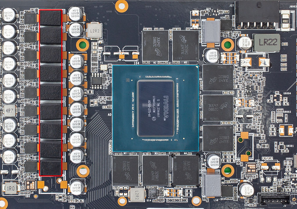
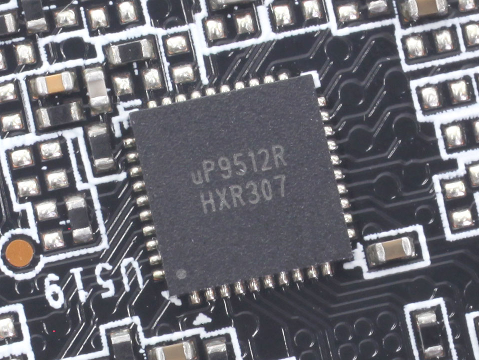
GPU voltage is a nine-phase design, managed by a uPI uP9512R controller.

OnSemi NCP302150 DrMOS components are used for GPU voltage; they are rated for 50 A of current each.
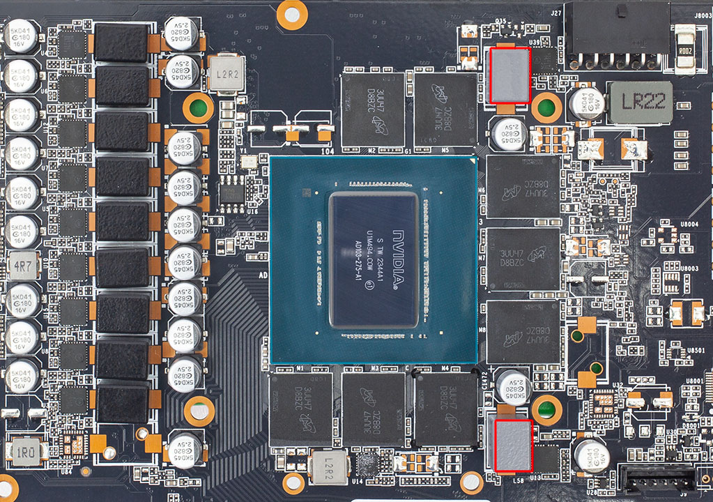

Memory voltage is a two-phase design, managed by a uPI uP9529Q controller.

For memory, OnSemi NCP302150 DrMOS with a 50 A rating are used, too.
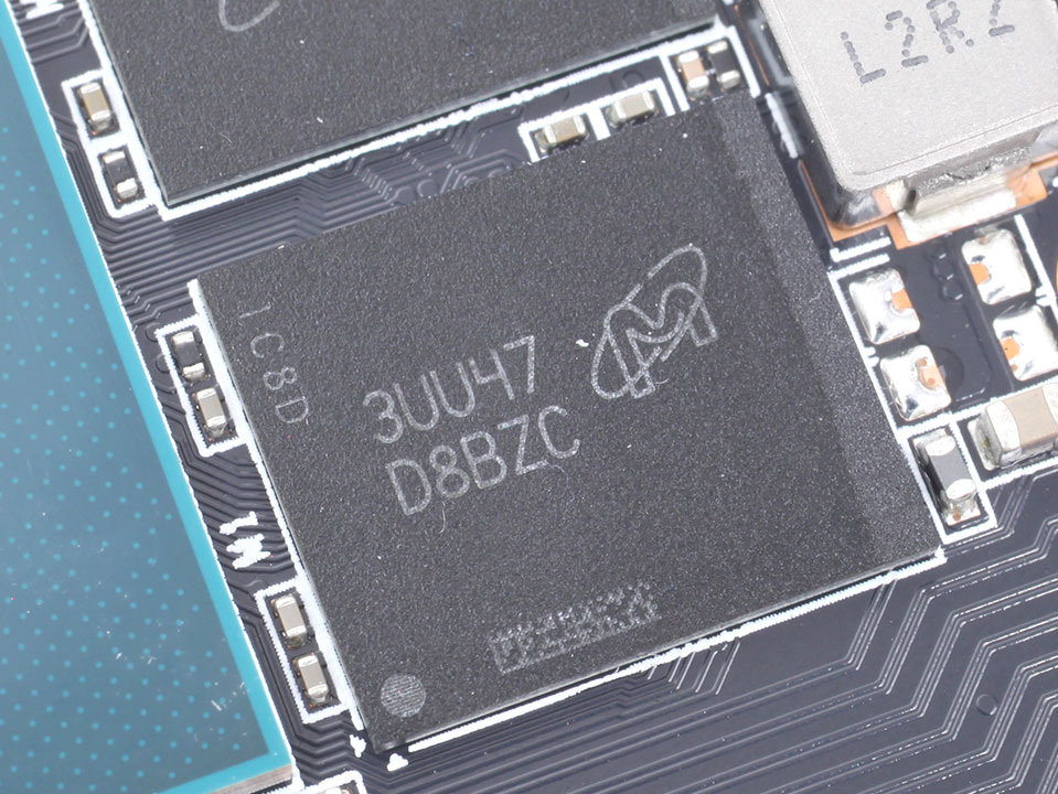
The GDDR6X memory chips are made by Micron and carry the model number D8BZC, which decodes to MT61K512M32KPA-21:U. They are specified to run at 1313 MHz (21 Gbps GDDR6 effective).
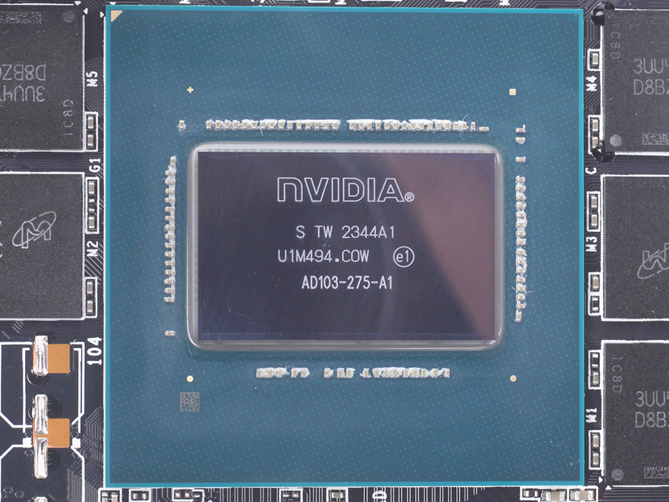
NVIDIA's AD103 graphics processor is the company's second Ada Lovelace GPU. It is built using a 5 nanometer process at TSMC Taiwan, with a transistor count of 45.9 billion and a die size of 379 mm².
May 13th, 2024 15:11 EDT
change timezone
Latest GPU Drivers
New Forum Posts
- [Reuters] 'Smile with your eyes': How to beat South Korea's AI hiring bots and land a job (7)
- Which Audio System Would you Choose and Why? (18)
- Which RAM for AMD 7950X3D (6)
- Purchased an AX1200i PSU as part of some forward planning, what tier is this PSU? (85)
- PKG Power much higher than usual (7)
- 2024 and STILL no dark mode? (43)
- Results and questions (6)
- Dell Workstation Owners Club (3083)
- How to optimize my PC by overclocking my system (16)
- What's the best tube I can get for Schiit Vali 3 headphone amp under $30? (5)
Popular Reviews
- ZMF Caldera Closed Planar Magnetic Headphones Review
- Homeworld 3 Performance Benchmark Review - 35 GPUs Tested
- Corsair MP700 Pro SE 4 TB Review
- Bykski CPU-XPR-C-I CPU Water Block Review - Amazing Value!
- ThundeRobot ML903 NearLink Review
- Upcoming Hardware Launches 2023 (Updated Feb 2024)
- AMD Ryzen 7 7800X3D Review - The Best Gaming CPU
- CHERRY XTRFY M64 Pro Review
- ASUS Radeon RX 7900 GRE TUF OC Review
- Corsair iCUE Link RX120 RGB 120 mm Fan Review
Controversial News Posts
- Intel Statement on Stability Issues: "Motherboard Makers to Blame" (266)
- AMD to Redesign Ray Tracing Hardware on RDNA 4 (224)
- Windows 11 Now Officially Adware as Microsoft Embeds Ads in the Start Menu (172)
- NVIDIA to Only Launch the Flagship GeForce RTX 5090 in 2024, Rest of the Series in 2025 (152)
- Sony PlayStation 5 Pro Specifications Confirmed, Console Arrives Before Holidays (119)
- AMD Hits Highest-Ever x86 CPU Market Share in Q1 2024 Across Desktop and Server (114)
- AMD's RDNA 4 GPUs Could Stick with 18 Gbps GDDR6 Memory (114)
- AMD Ryzen 9 7900X3D Now at a Mouth-watering $329 (104)