 27
Palit GeForce RTX 5070 GamingPro OC Review
Test Setup »High-resolution PCB Pictures
These pictures are for the convenience of volt modders and people who would like to see all the finer details on the PCB. Feel free to link back to us and use these in your articles, videos or forum posts.

High-resolution versions are also available (front, back).
Circuit Board (PCB) Analysis


A 9-phase VRM powers the GPU, highlighted in the red rectangles above. These are controlled by an Alpha & Omega AOZ73004CQI (ENC0) voltage controller.

All GPU power phases use Alpha & Omega AOZ5311NQI-03 (BLN3) DrMOS with a rating of 55 A.
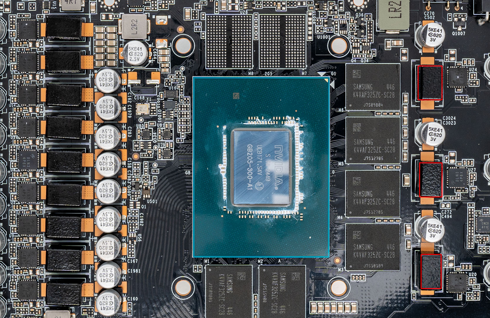

Powering the six GDDR7 memory chips is a 3-phase VRM driven by another Alpha & Omega AOZ73004CQI voltage controller.

Just like GPU, the memory is handled by Alpha & Omega AOZ5311NQI-03 (BLN3) DrMOS rated for 55 A.

The GDDR7 memory chips are made by Samsung, and bear the model number K4VAF325ZC-SC28, they are rated for 28 Gbps.

The NVIDIA GB205 GPU at the heart of the GeForce RTX 5070 is much smaller than the chip used on the RTX 5080 and RTX 5090. It is fabricated using a 5 nanometer "NVIDIA 4N" process at TSMC Taiwan (same process as Ada). The die measures 263 mm², and comes with a transistor count of 31.1 billion.
Nov 22nd, 2026 17:42 CST
change timezone
Latest GPU Drivers
New Forum Posts
- What are you playing? (26240)
- UPS what one to get? (48)
- Honestly, do you care about GTA VI? (265)
- Your PC ATM (36458)
- Gacha Games - Discussions, Pulls, Updates, etc. (1157)
- Last game you purchased? (1414)
- Making a game in Godot engine (19)
- Intel D270 (5)
- X870E AORUS ELITE WIFI7 thread with setting and OC (69)
- Gigabyte Aorus Master X570 settings / 7900XTX / 5950x /32GB Samsung B-die (13)
Popular Reviews
- Microsoft Surface Laptop Ultra Review - The Next-gen Arm Laptop
- Corsair RM1200e (Second Generation) Review
- Pulsar Office Tour & First Look at P1 Dual-Sensor Mouse
- Upcoming Hardware Launches 2027 (Updated Nov 2026)
- Ugreen NASync DXP4800 GT Review
- AMD Ryzen 7 9800X3D Review - The Best Gaming Processor
- Biwin Black Opal NV7400 2 TB Review
- AMD Zen 6 Technical Deep Dive
- Phantom Blade Zero Performance Benchmark Review - 35 GPUs Tested
- AMD Ryzen 7 5800X3D 10th Anniversary Review
TPU on YouTube
Controversial News Posts
- NVIDIA Co-Founder and CEO Jensen Huang Officially Resigns (492)
- Report: Jensen Huang Eyes NVIDIA Comeback (266)
- Open Letter Asking NVIDIA to Reinstate Jensen Huang Passes 115,000 Signatures (184)
- OpenAI CEO Argues Home PCs Waste the World's Limited DRAM Supply (152)
- NVIDIA Launches Investigation Into Jensen Huang's Relationship With Suspected Chinese Spy (136)
- Intel "Raptor Lake Next" 16-Core and 20-Core CPUs Surface (130)
- NVIDIA GeForce RTX 50-Series Scheduled for up to $500 Price Hike This Week (89)
- Intel Razor Lake Gets a 12 P-Core bLLC Chip With No E-Cores, Per Leak (86)