 55
Phison E28 PCIe 5.0 SSD Engineering Sample Review - Efficiency Magic
Test Setup »The Drive
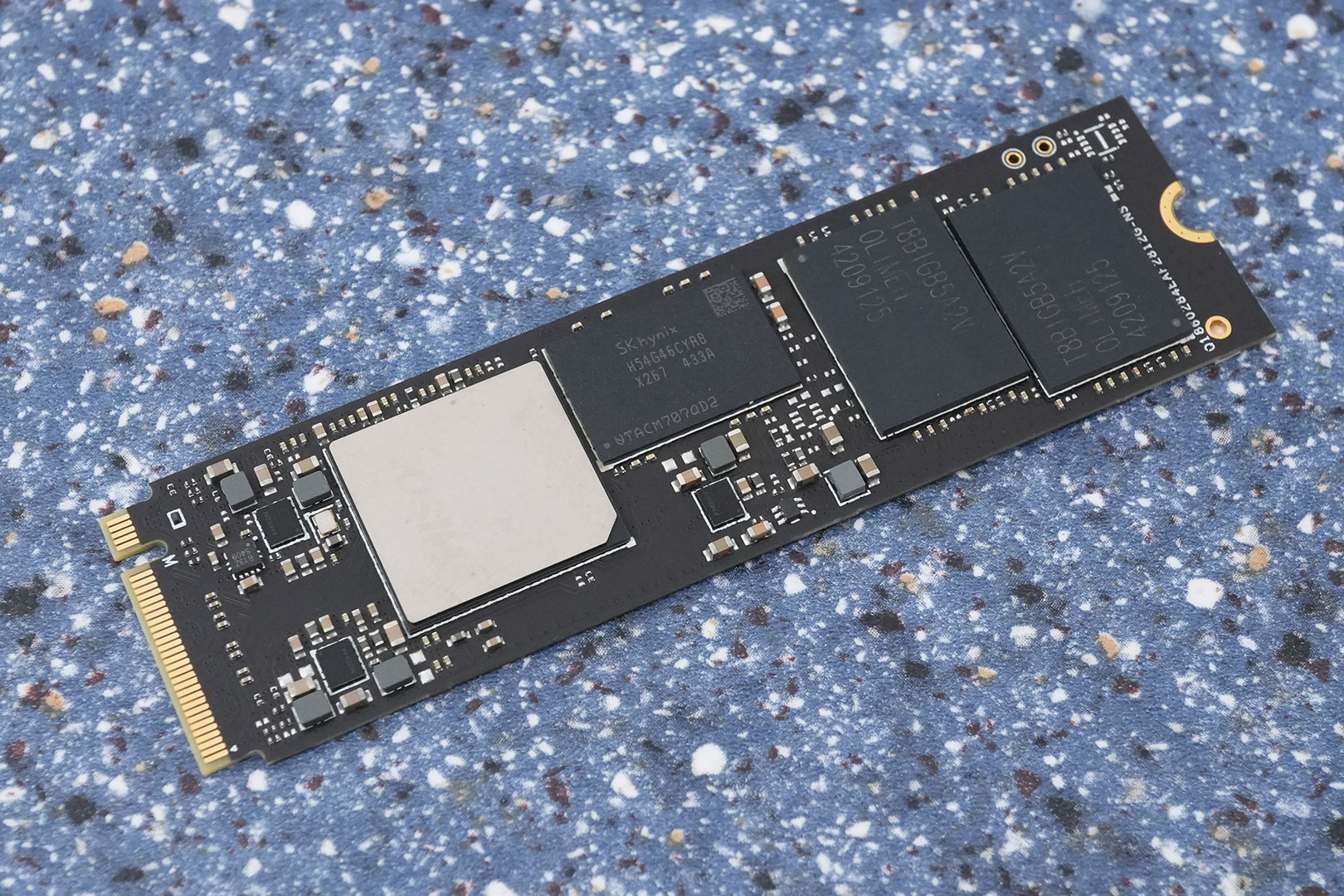

The drive is designed for the M.2 2280 form factor, which makes it 22 mm wide and 80 mm long.
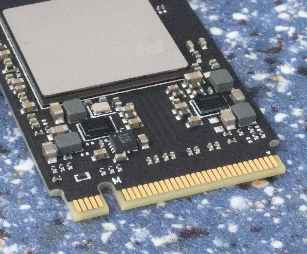
PCI-Express 5.0 x4 is used as the host interface to the rest of the system, which doubles the theoretical bandwidth compared to PCIe 4.0 x4.
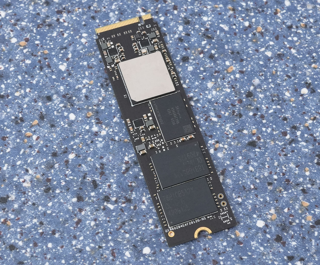
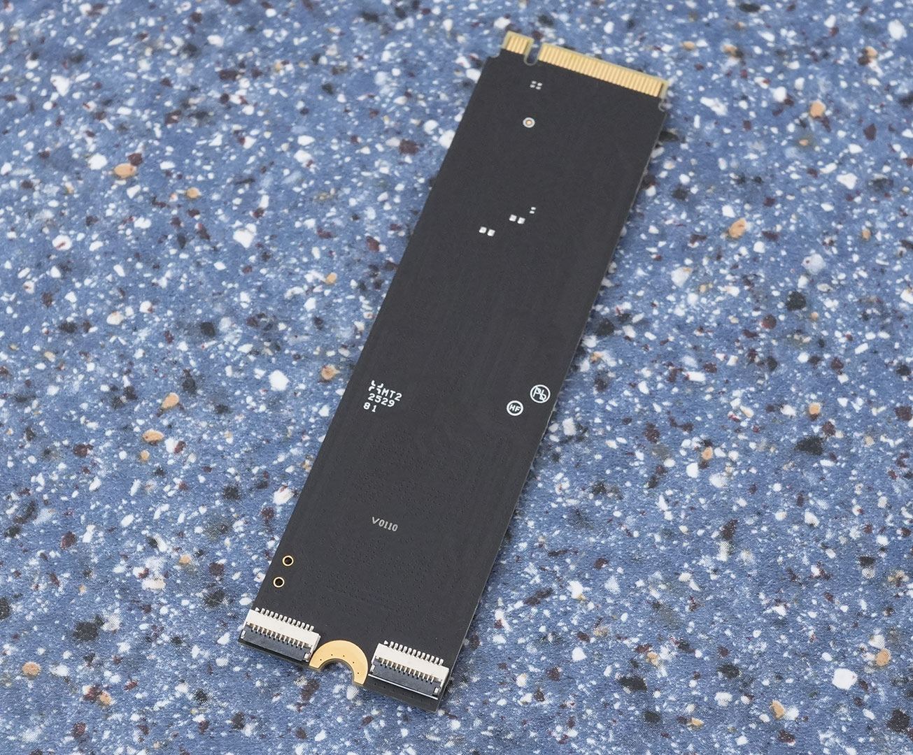
On the PCB you'll find the controller, two flash chips and a DRAM cache chip.

Just like on their other recent controllers, Phison ensured that the Z-Height of the controller package matches the NAND flash height, ensuring an even heatsink application. As a result, the DRAM cache doesn't come into contact with the heatsink, which is not an issue because it doesn't get very hot.
Chip Component Analysis
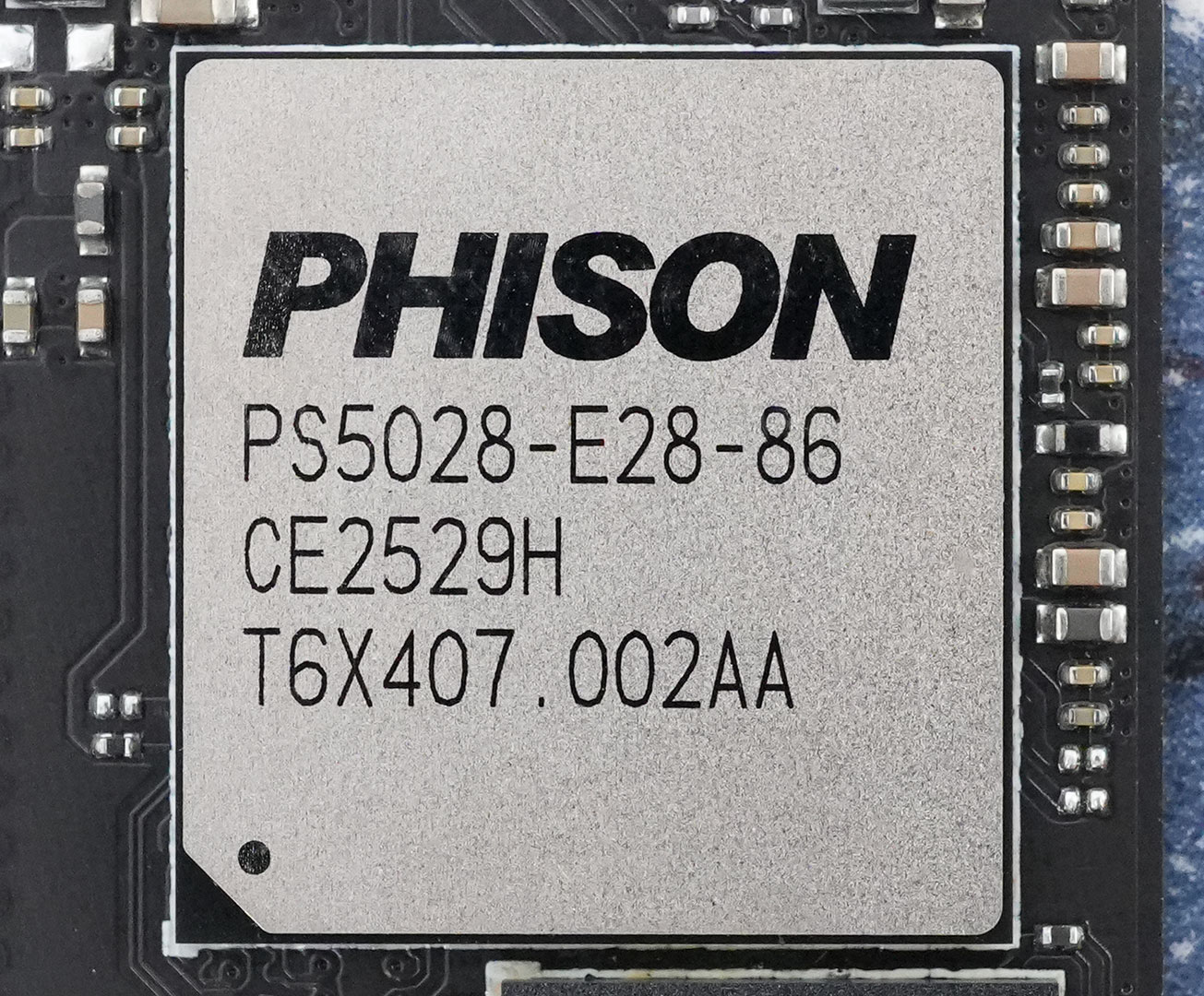
The Phison E28 controller is the third PCI-Express 5.0 controller developed by the company for consumer purposes. It succeeds the high-end E26, providing PCIe 5.0 x4 support and utilizing eight flash channels. Phison is fabricating the controller using a 6 nanometer process at TSMC Taiwan.

The two flash chips are Kioxia BiCS8 218-layer 3D TLC NAND. Each chip has a capacity of 1 TB.
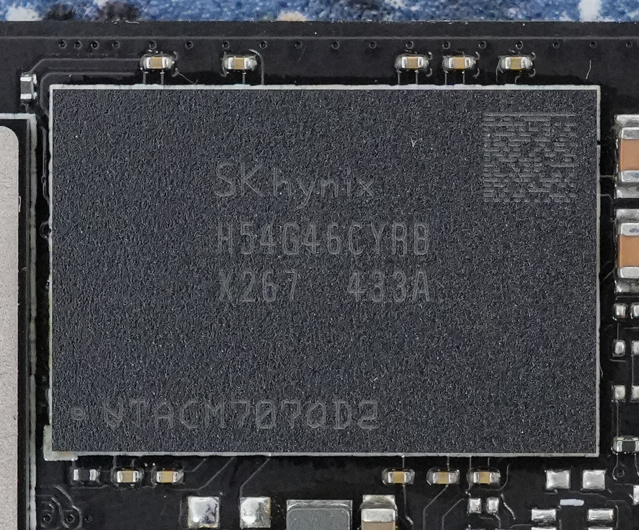
The Hynix DRAM cache chip has a capacity of 2 GB and runs at LPDDR4-4266.
Nov 16th, 2026 07:39 CST
change timezone
Latest GPU Drivers
New Forum Posts
- Without Jensen, PC gaming will be (3)
- Folding Pie and Milestones!! (10206)
- The Official Linux/Unix Desktop Screenshots Megathread (915)
- GPU Temperatures Rise Very Quickly in FurMark – Is This Normal? (17)
- Can you guess Which game it is? (327)
- no OpenGL showing support when... (11)
- The Official Thermal Interface Material thread (2302)
- no "PhysX" workable (15)
- Asus Maximus hero z890 latest Bios 3410 (0)
- What can the FX 8320 do today? Here is the answer. (63)
Popular Reviews
- ASUS ROG Strix B850-I Gaming Wi-Fi7 W Review
- Corsair HX1000i Shift Crystal Review
- AMD Zen 6 Technical Deep Dive
- Upcoming Hardware Launches 2027 (Updated Nov 2026)
- Montech King 95 3D PRO Review
- NZXT C1200 Platinum Review
- Phantom Blade Zero Performance Benchmark Review - 35 GPUs Tested
- AMD Ryzen 7 9800X3D Review - The Best Gaming Processor
- NZXT H7 RGB+ Review
- NZXT H5 Review
TPU on YouTube
Controversial News Posts
- NVIDIA Co-Founder and CEO Jensen Huang Officially Resigns (431)
- Open Letter Asking NVIDIA to Reinstate Jensen Huang Passes 115,000 Signatures (184)
- OpenAI CEO Argues Home PCs Waste the World's Limited DRAM Supply (152)
- NVIDIA Launches Investigation Into Jensen Huang's Relationship With Suspected Chinese Spy (136)
- Intel "Raptor Lake Next" 16-Core and 20-Core CPUs Surface (130)
- Legendary Game Studio BioWare Shuts Down Following EA Layoffs (104)
- Dell CEO Says the Memory Shortage Will Get Worse in 2027 (95)
- NVIDIA GeForce RTX 50-Series Scheduled for up to $500 Price Hike This Week (89)