 48
48
Sapphire HD 7970 Toxic 6 GB Review
Test Setup »A Closer Look


Sapphire's cooler uses a large copper vapor chamber to soak up heat from the GPU surface. You can also see the thermal pads that cool the memory chips on the front side of the GPU.

Once we remove the main heatsink, you can see many smaller heatsinks that keep voltage-regulation circuitry cool.
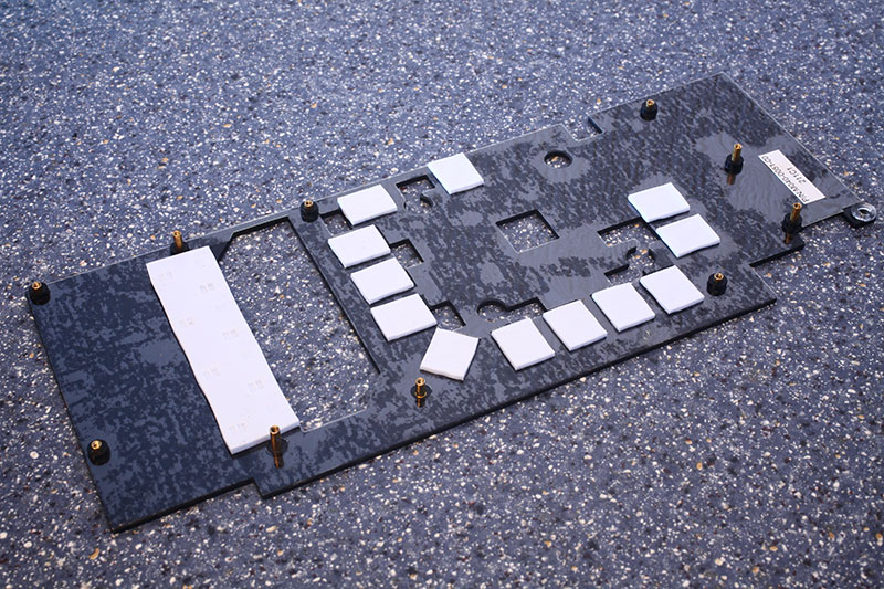
Sapphire has also installed a metal backplate that cools the memory chips on the back side and has an additional thermal pad to help with VRM cooling.
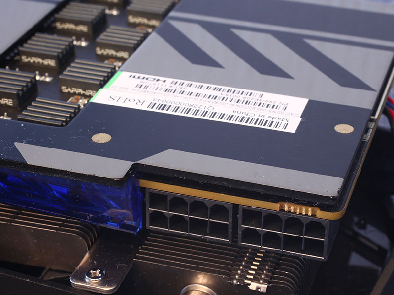
The card requires two 8-pin PCI-Express power cables for operation. This power configuration is good for up to 375 W of power draw.
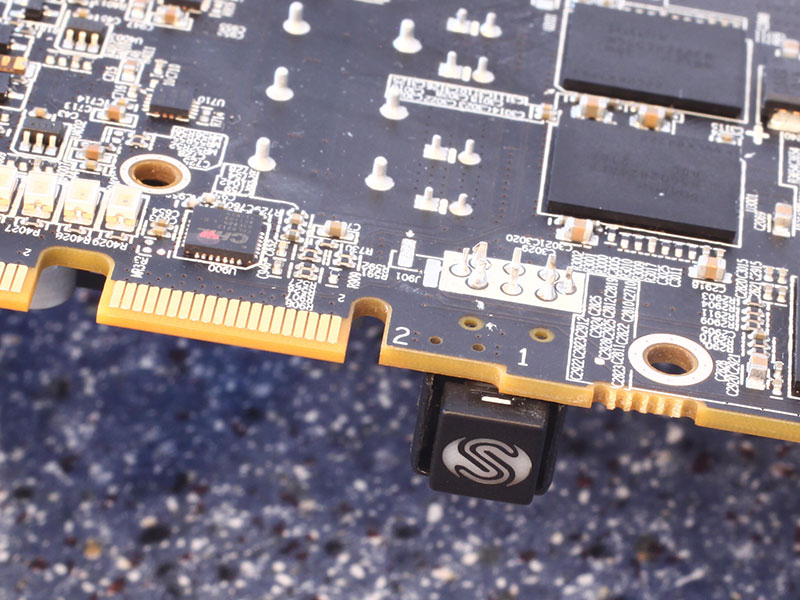
This button located near the CrossFire connectors, switches between two BIOSes on the card. On other HD 7900 Series cards, this dual BIOS feature acts just as a safeguard against problems during BIOS flashing. On the Sapphire Toxic, this feature has been extended to provide a BIOS that runs clocks beyond Sapphire's default clock for the HD 7970 at higher voltage, to ensure stability, which will influence power/heat/noise.

For voltage control the card uses a CHiL CHL8228G, which is a common voltage controller nowadays. It offers software voltage control, comprehensive monitoring features, and is well supported by most overclocking software.

The GDDR5 memory chips are made by Hynix and carry the model number H5GQ2H24MFR-R0C. They are specified to run at 1500 MHz (6000 MHz GDDR5 effective).

AMD's Tahiti graphics processor introduced the GCN shader architecture. it is also the first GPU to be produced on a 28 nm process at TSMC. The transistor count is 4.31 billion.
May 4th, 2024 21:22 EDT
change timezone
Latest GPU Drivers
New Forum Posts
- Apparently Valve is giving refunds on Helldivers 2 regardless of hour count. Details inside. (20)
- Post your 7zip 23.01 scores (16)
- Is updating BIOS to beta versions a good idea if you have the most recent version installed but still face issues? (3)
- Everytime i plug something into my wall, it stutters, and it never goes away (6)
- Unigine Heaven 4.0 Benchmark Scores Part 2 (930)
- Change GPU or PSU ? Games looks bad with microsuttering (13)
- Only some humans can see refresh rates faster than others, I am one of those humans. (100)
- Have you got pie today? (16326)
- WCG Daily Numbers (12506)
- TPU's Rosetta Milestones and Daily Pie Thread (1870)
Popular Reviews
- Finalmouse UltralightX Review
- Meze Audio LIRIC 2nd Generation Closed-Back Headphones Review
- ASRock NUC BOX-155H (Intel Core Ultra 7 155H) Review
- Montech Sky Two GX Review
- Upcoming Hardware Launches 2023 (Updated Feb 2024)
- Cougar Hotrod Royal Gaming Chair Review
- Alienware Pro Wireless Gaming Keyboard Review
- HYTE THICC Q60 240 mm AIO Review
- AMD Ryzen 7 7800X3D Review - The Best Gaming CPU
- Logitech G Pro X Superlight 2 Review - Updated with 4000 Hz Tested
Controversial News Posts
- Intel Statement on Stability Issues: "Motherboard Makers to Blame" (237)
- Windows 11 Now Officially Adware as Microsoft Embeds Ads in the Start Menu (167)
- AMD to Redesign Ray Tracing Hardware on RDNA 4 (130)
- Sony PlayStation 5 Pro Specifications Confirmed, Console Arrives Before Holidays (117)
- AMD's RDNA 4 GPUs Could Stick with 18 Gbps GDDR6 Memory (114)
- NVIDIA Points Intel Raptor Lake CPU Users to Get Help from Intel Amid System Instability Issues (106)
- AMD "Strix Halo" Zen 5 Mobile Processor Pictured: Chiplet-based, Uses 256-bit LPDDR5X (103)
- AMD Ryzen 9 7900X3D Now at a Mouth-watering $329 (103)