 60
60
Sapphire Radeon RX 5700 XT Pulse Review
(60 Comments) »Introduction
Sapphire today launched Radeon RX 5700 XT Pulse, its first custom-design RX 5700 XT Navi graphics card. The Pulse series of graphics cards from Sapphire are positioned as high cost-performance products, just below its premium Nitro series. Priced close to the $400 baseline AMD asks for this GPU, the RX 5700 XT Pulse combines a custom-design PCB with similar VRM chops to the AMD reference design, but tops it with a dual BIOS and the much sought after idle=fan-stop feature. This launch by Sapphire comes a little over a month since AMD's 7th July debut of the RX 5700 Navi series.
The Radeon RX 5700 XT is AMD's first true performance-segment graphics card in over two years since the RX Vega series. It's based on the brand new "Navi" architecture that leverages the 7 nm silicon fabrication process and brand new number-crunching machinery AMD calls RDNA compute units. These constitute the biggest update to AMD's GPU design since the very first Graphics CoreNext (GCN) architecture circa 2013. Together with clock speeds, RDNA is designed to bring about massive IPC improvements over GCN. The silicon also has a number of architectural changes. An interesting series of price adjustments and product launches ensures that even at its starting price of $399, it offers a bit more price-performance than NVIDIA.
AMD had originally planned to launch the Radeon RX 5700 XT at $449 and the RX 5700 at $399, with the two cards beating the $499 NVIDIA RTX 2070 and $349 RTX 2060, respectively. This forced NVIDIA to refresh its lineup with the new RTX 2070 Super at $499 and the RTX 2060 Super at $399. The RTX 2060 Super in particular was carefully crafted not to cannibalize the RTX 2070. AMD seeped into this imbroglio of NVIDIA and slotted the RX 5700 XT at $399 and the RX 5700 at $349, at which they outclass the RTX 2060 Super and original RTX 2060, respectively. NVIDIA didn't adjust prices of its RTX 2060 Super or RTX 2070 Super any further, and we hence have a fair bit of headroom between the RTX 2060 Super and RTX 2070 Super, in which AMD's board partners can launch custom-design RX 5700 XT cards with factory-overclocked speeds and other goodies, such as quieter coolers.
At the heart of the Radeon RX 5700 XT is the 7 nm "Navi 10" silicon with an impressive 10.3 billion transistors crammed into a 251 mm² die. Unlike the "Vega 20," Navi is a more traditional GPU in that the package only has the GPU die and is surrounded by memory chips. AMD opted for cost-effective 256-bit GDDR6 memory over exotic design choices such as HBM2. At a memory frequency of 14 Gbps, Navi enjoys a healthy memory bandwidth of 448 GB/s. It also features the latest-generation PCI-Express gen 4.0 x16 host interface with full backwards compatibility for older generations of PCIe, which means you can pair it with AMD's new Ryzen 3000 processors on an X570 chipset motherboard. The buzz-words "7 nm" and "PCIe gen 4.0" are extensively used in AMD's marketing, as if to suggest that Navi is a generation ahead of NVIDIA's Turing, which is built on 12 nm and has PCIe gen 3.0.
The Sapphire Radeon RX 5700 XT Pulse features a custom-design PCB that has similar specs to the AMD reference PCB with its 7+2 phase setup, but a significantly different design with a different combination of a VRM controller and components. The dual-BIOS feature protects you from bad BIOS flashing. There's also a reasonable factory overclock with 1925 MHz maximum boost frequency to be had. The cooling solution features an aluminium fin-stack heatsink ventilated by a pair of fans that turn off when the GPU is idling. At a price of $410, the card is only $10 pricier than the AMD reference design.
| Price | Shader Units | ROPs | Core Clock | Boost Clock | Memory Clock | GPU | Transistors | Memory | |
|---|---|---|---|---|---|---|---|---|---|
| GTX 1070 Ti | $450 | 2432 | 64 | 1607 MHz | 1683 MHz | 2000 MHz | GP104 | 7200M | 8 GB, GDDR5, 256-bit |
| RTX 2060 | $290 | 1920 | 48 | 1365 MHz | 1680 MHz | 1750 MHz | TU106 | 10800M | 6 GB, GDDR6, 192-bit |
| RX 5700 | $350 | 2304 | 64 | 1465 MHz | 1625 MHz | 1750 MHz | Navi 10 | 10300M | 8 GB, GDDR6, 256-bit |
| GTX 1080 | $500 | 2560 | 64 | 1607 MHz | 1733 MHz | 1251 MHz | GP104 | 7200M | 8 GB, GDDR5X, 256-bit |
| RTX 2060 Super | $400 | 2176 | 64 | 1470 MHz | 1650 MHz | 1750 MHz | TU106 | 10800M | 8 GB, GDDR6, 256-bit |
| RX Vega 64 | $400 | 4096 | 64 | 1247 MHz | 1546 MHz | 953 MHz | Vega 10 | 12500M | 8 GB, HBM2, 2048-bit |
| GTX 1080 Ti | $700 | 3584 | 88 | 1481 MHz | 1582 MHz | 1376 MHz | GP102 | 12000M | 11 GB, GDDR5X, 352-bit |
| RX 5700 XT | $400 | 2560 | 64 | 1605 MHz | 1755 MHz | 1750 MHz | Navi 10 | 10300M | 8 GB, GDDR6, 256-bit |
| Sapphire RX 5700 XT Pulse | $410 | 2560 | 64 | 1670 MHz | 1815 MHz | 1750 MHz | Navi 10 | 10300M | 8 GB, GDDR6, 256-bit |
| RTX 2070 | $440 | 2304 | 64 | 1410 MHz | 1620 MHz | 1750 MHz | TU106 | 10800M | 8 GB, GDDR6, 256-bit |
| RTX 2070 Super | $500 | 2560 | 64 | 1605 MHz | 1770 MHz | 1750 MHz | TU104 | 13600M | 8 GB, GDDR6, 256-bit |
| Radeon VII | $680 | 3840 | 64 | 1802 MHz | N/A | 1000 MHz | Vega 20 | 13230M | 16 GB, HBM2, 4096-bit |
| RTX 2080 | $630 | 2944 | 64 | 1515 MHz | 1710 MHz | 1750 MHz | TU104 | 13600M | 8 GB, GDDR6, 256-bit |
Architecture: Navi and RDNA

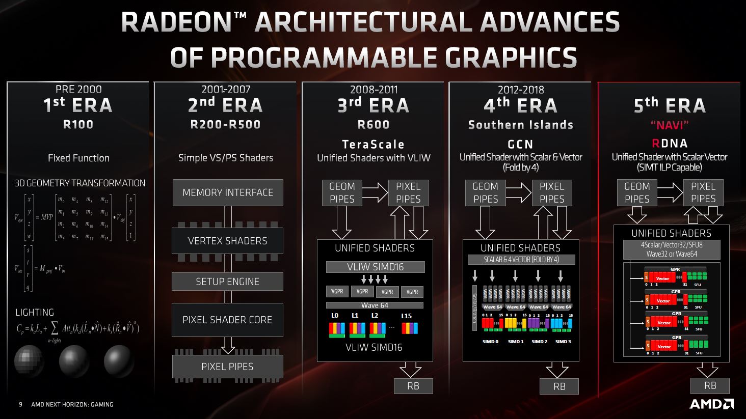
We've been hearing the moniker "Navi" for years now, and AMD threw another one at us this Computex, "RDNA", so let us demystify the two first. "Navi" is the codename for the family of silicon the GPU is based on. RDNA is a new architecture introduced by AMD to succeed Graphics Core Next (GCN). It prescribes the GPU's component hierarchy and, more importantly, its main number-crunching machinery, the compute units.
Another example of this distinction would be "Vega". Vega 10, Vega 20, and Vega 12 are pieces of silicon from the same family, while the GPU follows the 5th generation Graphics Core Next architecture governing even its compute units. Over many years, AMD made incremental updates to GCN, but this time, it claims that RDNA is sufficiently different from GCN to not be considered a new version, but rather a new hardware component that brings with it massive IPC gains over the previous generation.


The Radeon RX 5700 series is built around "Navi 10", an elegant little piece of silicon engineered on the 7 nm process at TSMC with 10.3 billion transistors crammed into a die measuring just 251 mm². The chip features a PCI-Express 4.0 x16 bus interface and a 256-bit wide GDDR6 memory interface. Infinity Fabric, which debuted on AMD's Ryzen CPUs, is extensively used as an on-die interconnect linking the various major components.
The bulk of AMD's engineering effort with RDNA has been to increase the number of dedicated resources to avoid starvation by fewer components waiting for access to a resource. The "Navi 10" silicon has two Shader Engines sharing a centralized Command Processor that distributes workloads, a Geometry Processor, and ACEs (asynchronous compute engines).


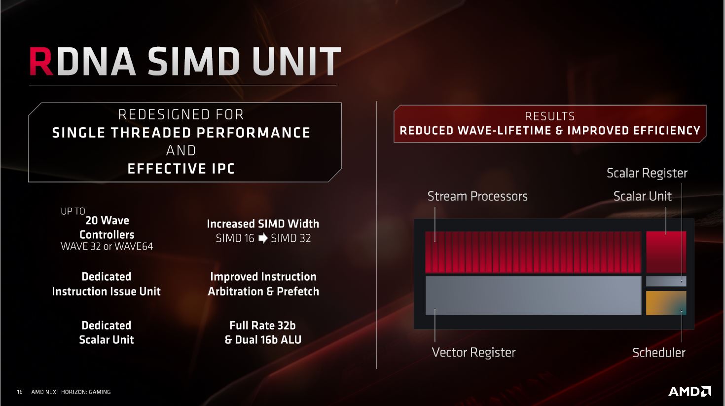
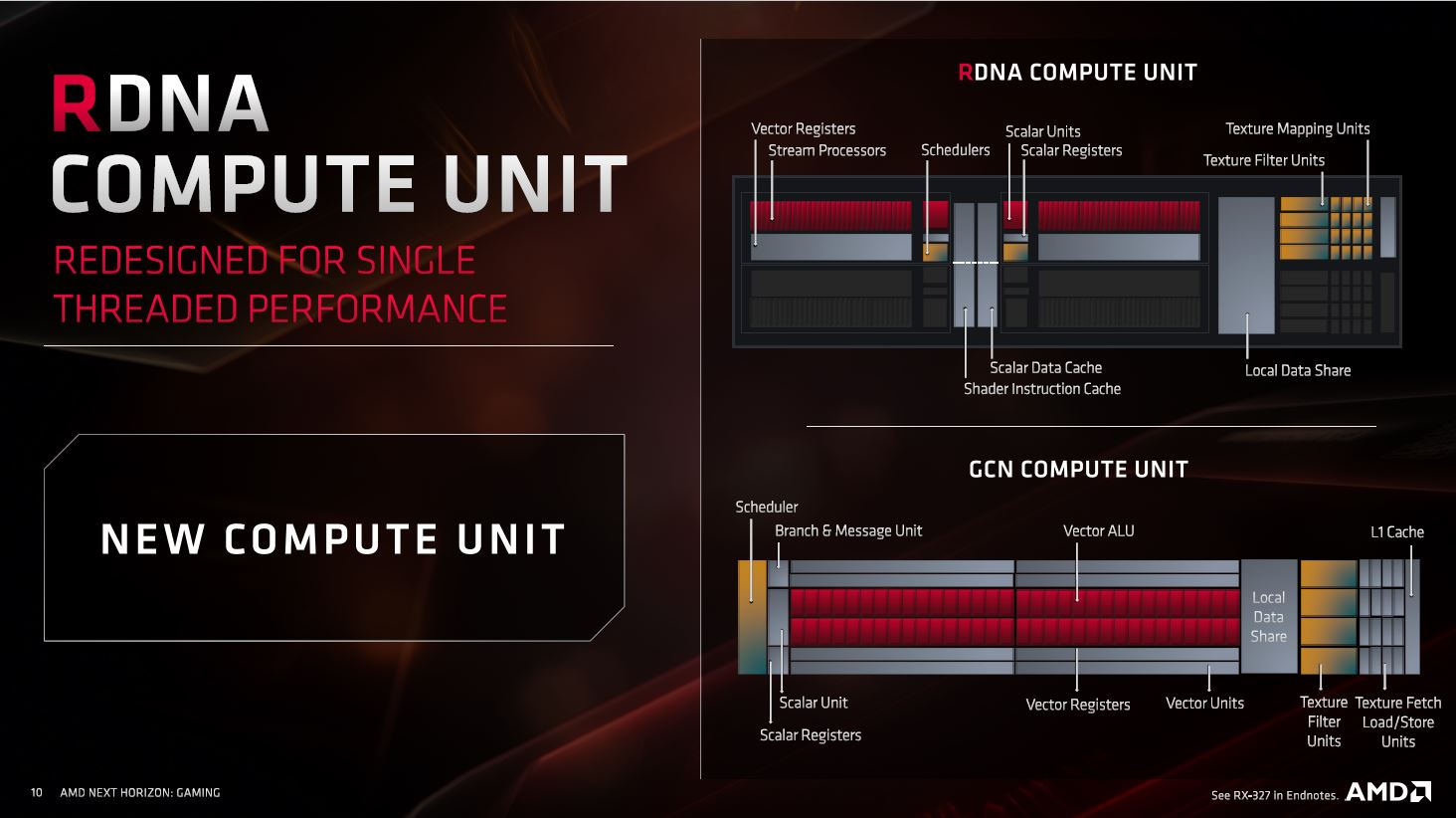
Each Shader Engine is further divided into two Graphics Engines. A graphics engine shares render backends, a Rasterizer, and a Prim Unit among five Workgroup Processors. This is where the core of RDNA begins. AMD figured it could merge two compute units (CUs) to share schedulers, scalar units, a data-share, instruction and data caches, and TMUs. The Workgroup Processor, or "dual-compute unit" as shown in the architecture block diagram, is for all intents and purposes indivisible in that individual CUs cannot be disabled.


An RDNA compute unit packs 64 stream processors for vector operations and double the number of scalar units for localized serial processing. The stream processors in a CU are split into groups of two, each equipped with a scalar unit. According to AMD, this greatly reduces latency and improves the overall IPC of the compute unit. It also more efficiently utilizes local caches.


The vector execution units, or stream processors, is where much of the GPU's parallel processing happens. Due to the redesigned compute unit, two scalar processors pull two SIMD32 vector units made up of 32 stream processors, each, instead of a single scalar processor pulling four SIMD16 vector units. How is this important? On GCN, the way SIMD units are laid out, all items in a Wave64 operation get to do work once every four clocks due to hardware interleaving. With RDNA, Wave32 work items can do work every clock cycle. In all, RDNA minimizes wasted clock cycles by more efficiently and uniformly utilizing the hardware resources.


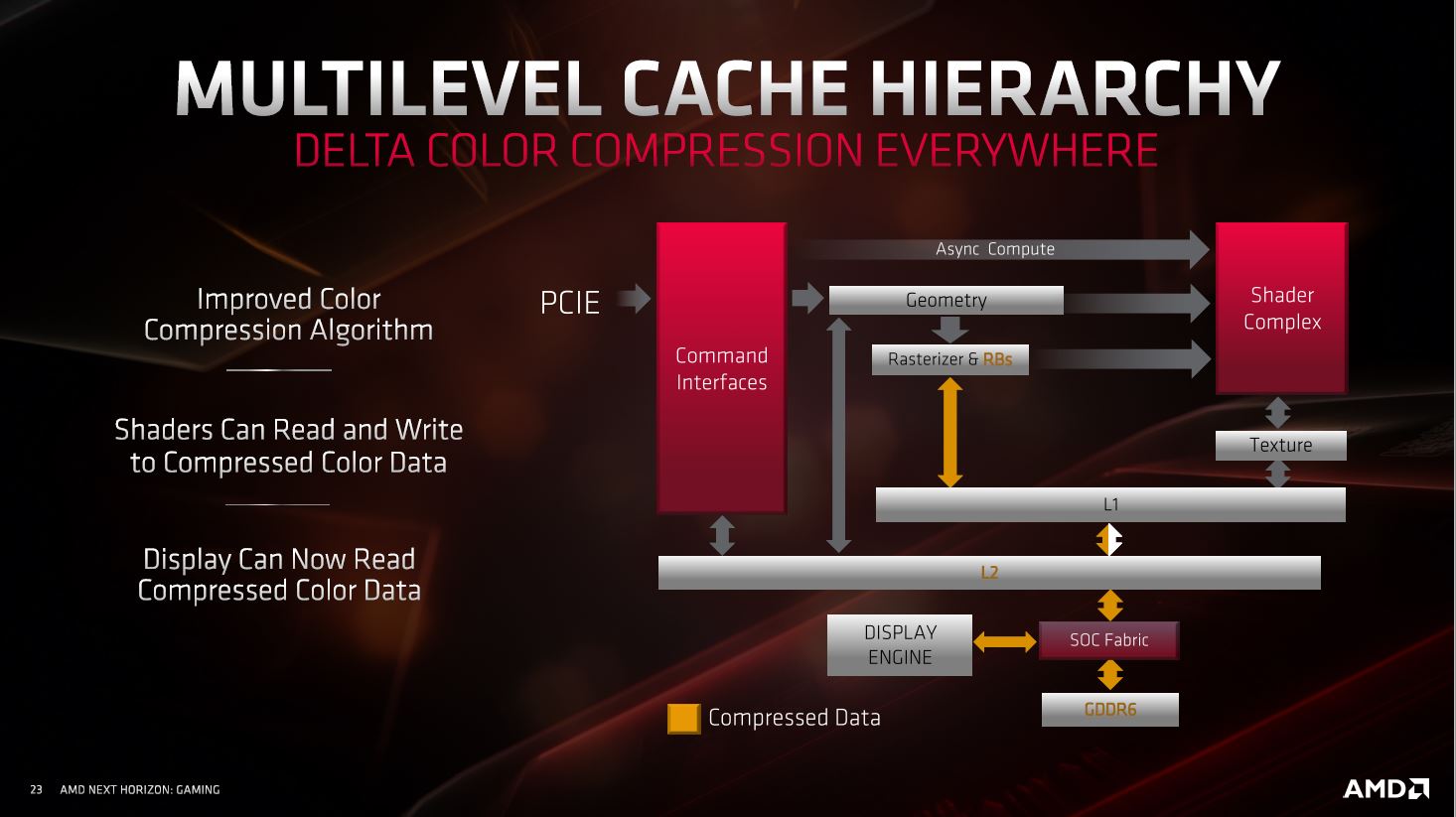
AMD examined previous generations of its graphics architecture to locate bottlenecks in the graphics pipeline. Besides increasing the number of dedicated resources, the company reworked the chip's cache hierarchy by cushioning data transfers at various stages. Each workgroup processor has dedicated 32 KB instruction and 16 KB data caches, which write back to a 128 KB L1 cache dedicated to each Graphics Engine.
These L1 caches talk to 4 MB of L2 cache. The introduction of the L1 cache and doubling in bandwidth between the various caches contributes greatly to IPC as it minimizes memory accesses, which are much slower than cache accesses. AMD is also using faster (lower latency) SRAM that reduces cache latencies by around 20 percent on die and by 8 percent at the memory level. AMD also introduced new features to the ACEs that include async-compute tunneling.
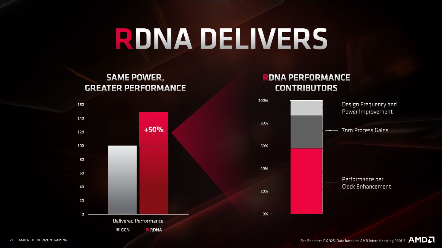
AMD summarizes the benefits of RDNA in a 25 percent IPC gain over the latest version of GCN, and an effective 50 percent performance gain for the GPU when taking into account IPC, the 7 nm process, and gains from the frequency and power management (ability to sustain boost frequencies better).
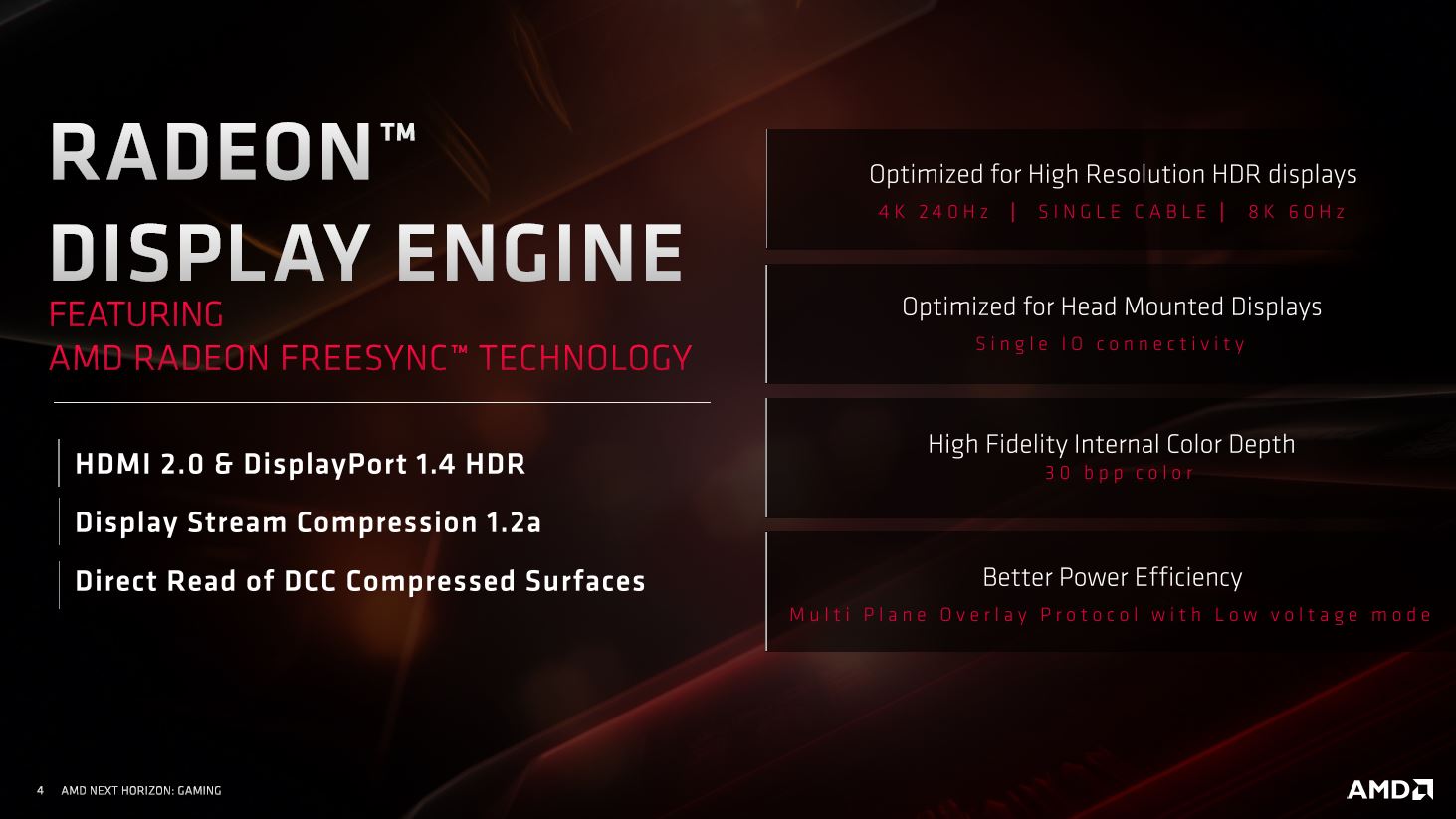

Elsewhere on the silicon, AMD updated the Display Engine and Multimedia Engine to keep up with the latest display and video standards. The Display Engine now supports DSC 1.2a (display stream compression) along with output standards HDMI 2.0 and DisplayPort 1.4 HDR to support display formats as bandwidth-intensive as 4K 240 Hz or 8K 60 Hz over a single cable, and 30 bits per pixel color depth. The multimedia engine supports VP9 and H.265 decoding at up to 8K 24 Hz, or 4K 90 Hz, and hardware-accelerated H.265 encoding at up to 4K 60 Hz.
Features: FidelityFX and Anti-Lag
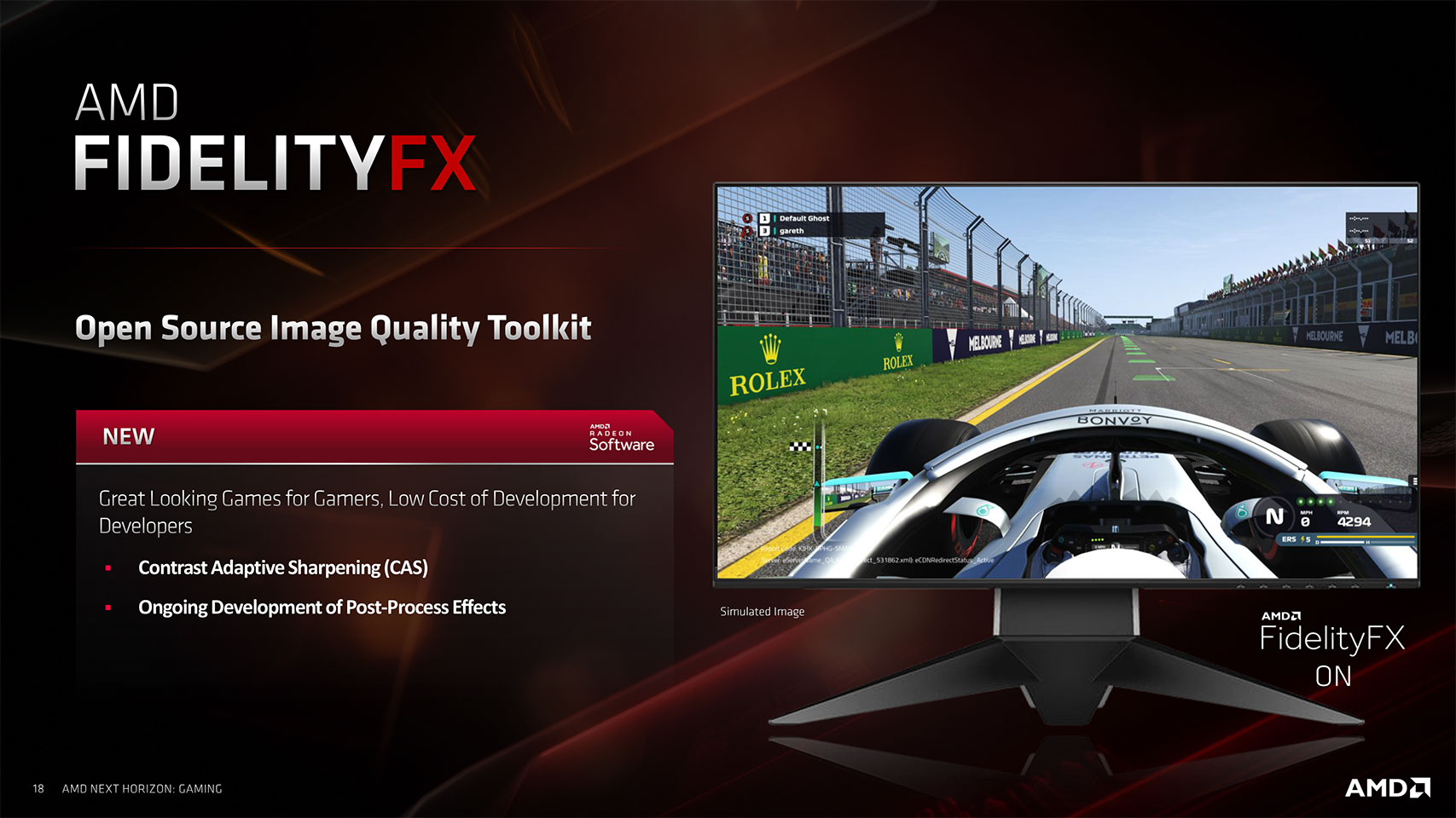


With each new graphics architecture, gamers expect new image quality enhancement features. NVIDIA introduced DLSS and AMD's response to that is FidelityFX, a combination of content-specific and image-specific quality enhancements. The first part of this is contrast-adaptive sharpening, which brings out details in a scene by enhancing their contrast. To work best, it requires game developers to declare which parts of the image are to be sharpened (like the HUD and on-screen texts). Details such as wear lines on the slick tires of a race car or hexagonal patterns on a wall come to life. We will test this feature later in a separate article.


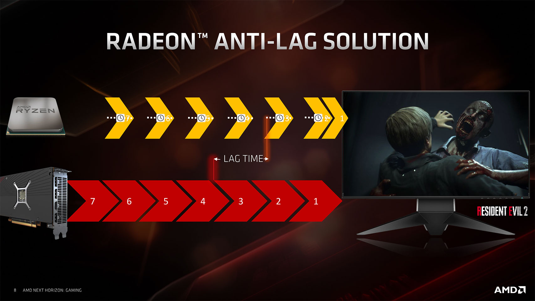
AMD wants to improve its adoption by professional e-Sports gamers by addressing a key bottleneck with modern high-end graphics: mouse lag. This would be the amount of time taken for a click to register and a response to be rendered by the GPU. Radeon Anti-Lag is a CTR (click-to-response) enhancement that reduced mouse lag by roughly a third across various popular e-Sports titles. This setting is effectively identical to "pre-rendered" frames on NVIDIA. Modern GPUs calculate one or two frames ahead, so they can better time sending them to the monitor to avoid stuttering. Of course, this results in input lag because any input information that comes in only makes it to the screen one or two frames later.
Packaging and Contents


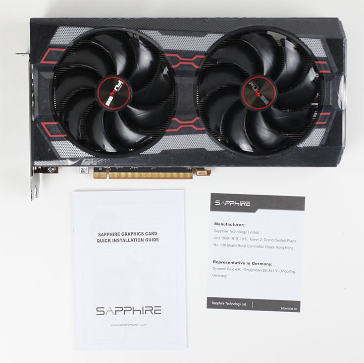
You will receive:
- Graphics card
- Documentation
The Card
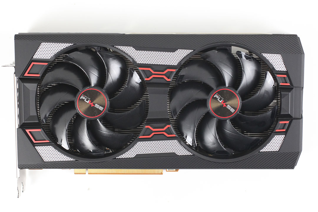
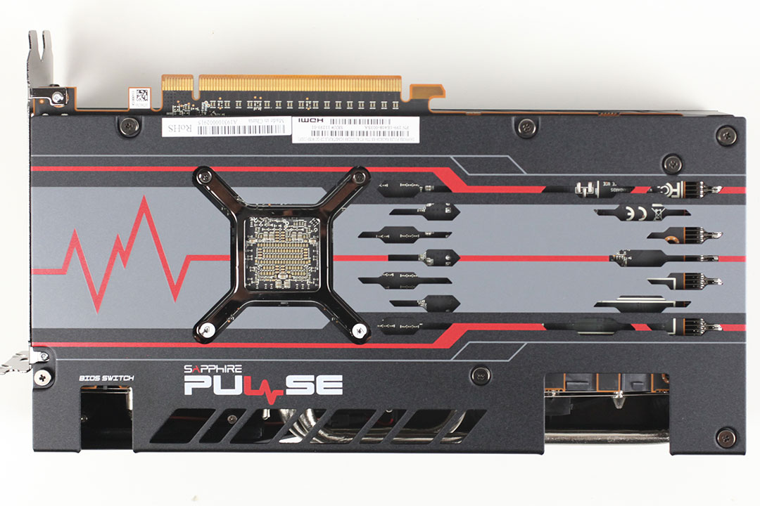
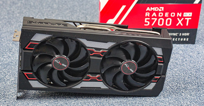
Sapphire's card uses relatively clean geometry paired with highlights in red and silver. The metal backplate explores the "Pulse" theme even further with a waveform resembling a heartbeat line. Dimensions of the card are 25.5 x 13.5 cm.

Installation requires a little bit over two slots in your system, so it's a three-slot card.

Display connectivity options include three standard DisplayPort 1.4a and an HDMI 2.0b.
AMD took the opportunity to update the display controllers handling these outputs by leveraging DSC 1.2a (display stream compression), which unlocks very high resolution and refresh-rate combinations over a single cable. Among the single-cable display modes supported are 8K 60 Hz (which took two DP 1.3 cables until now), 4K 240 Hz, and 1080p as high as 360 Hz. On top of these, the outputs support HDR and 30 bpc color-depth for better color accuracy in creative applications.
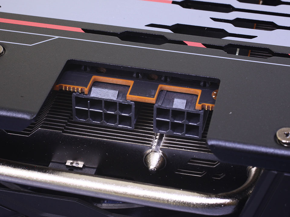
The board uses one 8-pin and one 6-pin power connector. This input configuration is specified for up to 300 watts of power draw.
AMD's Navi generation of GPUs no longer supports CrossFire. DirectX 12 does include its own set of multi-GPU capabilities, but the implementation requires game developers to put serious development time into a feature only a tiny fraction of their customers might ever use.
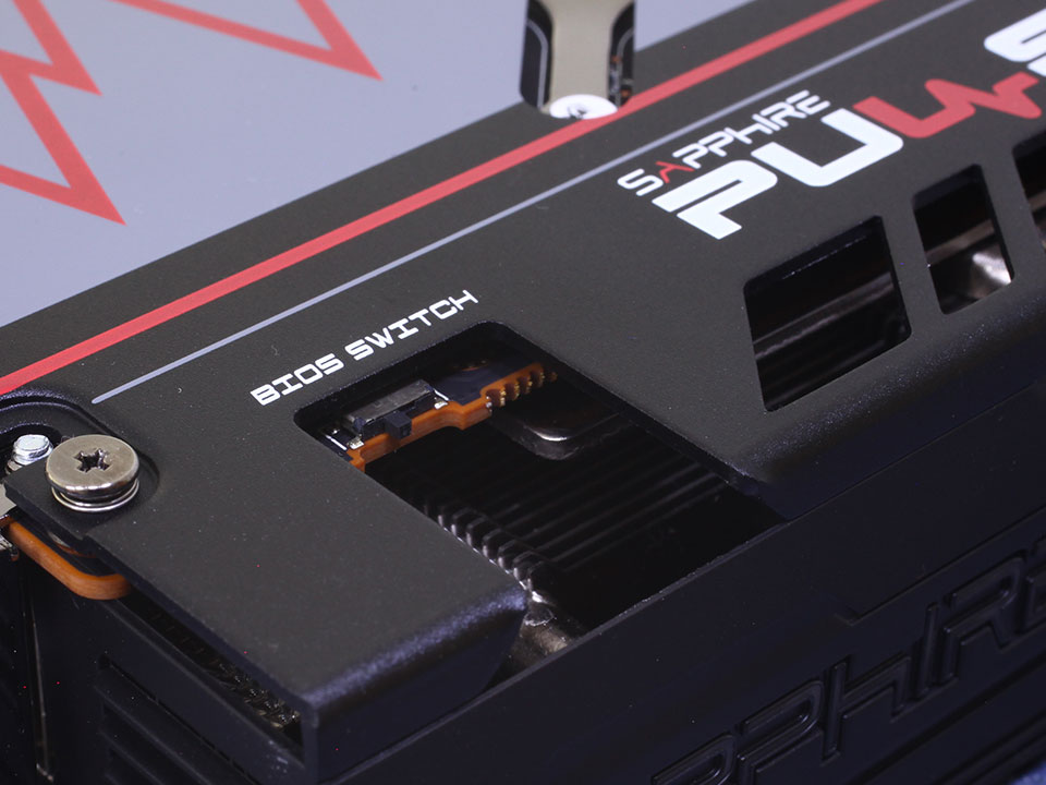
In this area, you'll also find a dual-BIOS switch, with the default setting being "Boost" and the other BIOS "Silent". It not only runs a quieter fan curve, but also comes with slightly lower clocks and voltages, which helps the card stay cool with even the reduced fan speeds.
Our Patreon Silver Supporters can read articles in single-page format.
May 10th, 2024 05:32 EDT
change timezone
Latest GPU Drivers
New Forum Posts
- Epic Games launcher's ridiculous CPU usage (36)
- Only some humans can see refresh rates faster than others, I am one of those humans. (241)
- not impressed - nvme vs ssd (77)
- What are you playing? (20608)
- RM750x (2021) enough for my 5800X3D + 7900XT system? (6)
- RTX 4070 vs RTX 4070 Ti power scaling (8)
- ALPHACOOL - ideas for IMPROVING products and NEW products (0)
- Battery swap for cyberpower UPS (67)
- Is hard drive sentinel trustworthy (9)
- What's a good option for a digital touchless thermometer? (19)
Popular Reviews
- CHERRY XTRFY M64 Pro Review
- Bykski CPU-XPR-C-I CPU Water Block Review - Amazing Value!
- Corsair iCUE Link RX120 RGB 120 mm Fan Review
- Corsair MP700 Pro SE 4 TB Review
- ThundeRobot ML903 NearLink Review
- Upcoming Hardware Launches 2023 (Updated Feb 2024)
- Finalmouse UltralightX Review
- AMD Ryzen 7 7800X3D Review - The Best Gaming CPU
- Sapphire Radeon RX 7700 XT Pure Review
- ASUS Radeon RX 7900 GRE TUF OC Review
Controversial News Posts
- Intel Statement on Stability Issues: "Motherboard Makers to Blame" (264)
- AMD to Redesign Ray Tracing Hardware on RDNA 4 (206)
- Windows 11 Now Officially Adware as Microsoft Embeds Ads in the Start Menu (169)
- NVIDIA to Only Launch the Flagship GeForce RTX 5090 in 2024, Rest of the Series in 2025 (144)
- Sony PlayStation 5 Pro Specifications Confirmed, Console Arrives Before Holidays (119)
- AMD's RDNA 4 GPUs Could Stick with 18 Gbps GDDR6 Memory (114)
- NVIDIA Points Intel Raptor Lake CPU Users to Get Help from Intel Amid System Instability Issues (106)
- AMD Ryzen 9 7900X3D Now at a Mouth-watering $329 (104)