 33
33
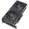
Sapphire Radeon RX 6600 XT Pulse OC Review
Test Setup »High-resolution PCB Pictures
These pictures are for the convenience of volt modders and people who would like to see all the finer details on the PCB. Feel free to link back to us and use these in your articles, videos or forum posts.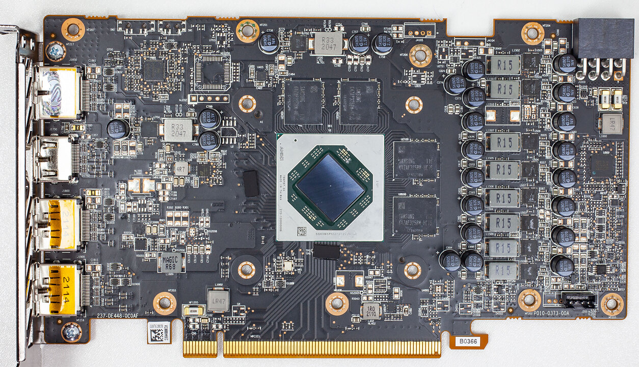

High-res versions are also available (front, back).
Circuit Board (PCB) Analysis


GPU voltage uses eight phases and is powered by an International Rectifier IR35217.

OnSemi NCP302155 DrMOS chips are used for the GPU voltage; they are rated for 55 A.


Memory voltage uses a two-phase design and is generated by an NCP81022N controller.

For memory, 45 A OnSemi NCP302045 DrMOS chips are used.

The GDDR6 chips are made by Samsung, carry the model number "K4ZAF325BM-HC16," and are rated to run at 16 Gbps.
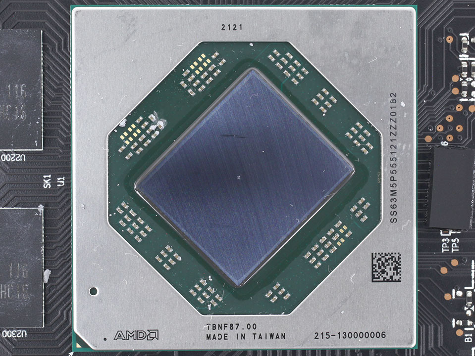
Built on the same TSMC N7 (7 nm) node as Navi 10, the Navi 23 silicon is spread across a 237 mm² die area and packs 11.6 billion transistors. The pinkish-red tinge we saw on Navi 10 is gone.
Apr 19th, 2024 20:56 EDT
change timezone
Latest GPU Drivers
New Forum Posts
- Roccat Kone AIMO has developed a double left click, when I click it once. Any fix out there? (35)
- I just succesfully baked DDR4 (71)
- Windows 11 General Discussion (5014)
- GTX 1060 6GB ASUS GPU Shuts Down after 5min of Gaming (4)
- Official Board Game Discussion (1)
- USB C to USB A hub (42)
- The Official Linux/Unix Desktop Screenshots Megathread (688)
- AMD RX 7000 series GPU Owners' Club (1068)
- I9 13890HX undervolting Suggestions (4)
- Undervolting Dell XPS 14 9440 is it possible? (7)
Popular Reviews
- Horizon Forbidden West Performance Benchmark Review - 30 GPUs Tested
- Fractal Design Terra Review
- Corsair 2000D Airflow Review
- Thermalright Phantom Spirit 120 EVO Review
- Minisforum EliteMini UM780 XTX (AMD Ryzen 7 7840HS) Review
- Creative Pebble X Plus Review
- FiiO KB3 HiFi Mechanical Keyboard Review - Integrated DAC/Amp!
- ASUS GeForce RTX 4090 STRIX OC Review
- NVIDIA GeForce RTX 4090 Founders Edition Review - Impressive Performance
- ASUS GeForce RTX 4090 Matrix Platinum Review - The RTX 4090 Ti
Controversial News Posts
- Sony PlayStation 5 Pro Specifications Confirmed, Console Arrives Before Holidays (111)
- NVIDIA Points Intel Raptor Lake CPU Users to Get Help from Intel Amid System Instability Issues (102)
- US Government Wants Nuclear Plants to Offload AI Data Center Expansion (98)
- AMD "Strix Halo" Zen 5 Mobile Processor Pictured: Chiplet-based, Uses 256-bit LPDDR5X (84)
- Windows 10 Security Updates to Cost $61 After 2025, $427 by 2028 (82)
- Developers of Outpost Infinity Siege Recommend Underclocking i9-13900K and i9-14900K for Stability on Machines with RTX 4090 (82)
- TechPowerUp Hiring: Reviewers Wanted for Motherboards, Laptops, Gaming Handhelds and Prebuilt Desktops (72)
- Intel Realizes the Only Way to Save x86 is to Democratize it, Reopens x86 IP Licensing (70)