 40
40
Sapphire Radeon RX 7900 XT Pulse Review
(40 Comments) »Introduction
Sapphire Radeon RX 7900 XT Pulse is among the most affordable custom-design RX 7000 RDNA 3 series graphics cards you can buy right now. The Pulse series from Sapphire represents a cost-effective product that's positioned close to the AMD reference design cards, but with superior thermals and more importantly, a quieter board design. The Radeon RX 7900 XT is the second-fastest RX 7000 series SKU, positioned a notch below the flagship RX 7900 XTX. AMD has looked to undercut NVIDIA's RTX 4080 with these cards, and has aggressively priced them in relation to the green team. The RX 7900 XT launched at $900, but its real-world pricing is now considerably below that with cards reaching $800, to match RTX 4070 Ti.

The Radeon RX 7900 XT has pretty much the same use-case as the flagship RX 7900 XTX: 4K Ultra HD gaming with maxed out settings. AMD claims generational improvements for the ray tracing performance of these cards, although you might want to step away from the presets and take control of a few settings to make ray traced games a bit more fluid at higher resolutions. The RX 7900 series debuts the new RDNA 3 graphics architecture that leverages the switch to the new 5 nm EUV foundry process, significantly higher shader counts, up to 17% IPC improvements for the shaders, and high clock speeds, to offer an over 50% performance/Watt gain over the previous generation, repeating the feat of the RX 6000 series RDNA2, which springboarded AMD back into the high-end PC graphics segment.
The new "Navi 31" GPU that the RX 7900 series is based on, debuts chiplets to GPUs—a method by which AMD can maximize its foundry allocation of the latest node, and save on costs. The company identified specific components of the GPU that don't benefit from the switch to 5 nm as much as the main graphics rendering machinery does—the memory controllers and last-level caches—and spun them off into tiny chiplets called the Memory Cache Dies (MCDs), built on the 6 nm process. There are six of these on Navi 31, each with a 64-bit GDDR6 memory interface, and a 16 MB segment of the GPU's Infinity Cache; which together make up the GPU's 384-bit GDDR6 memory bus, and 96 MB Infinity Cache.
While the flagship RX 7900 XTX maxes out Navi 31, by enabling all 96 RDNA 3 compute units, the RX 7900 XT is carved out of the silicon by enabling 84 out of 96 compute units, which work out to 5,376 stream processors, 80 2nd Gen Ray Accelerators that each offer a 50% ray intersection performance increase over the previous generation; 336 TMUs, and a mammoth 192 ROPs. While the RX 7900 XTX has 24 GB of 20 Gbps GDDR6 across the chip's full 384-bit memory interface, AMD gave the RX 7900 XT 20 GB of 20 Gbps GDDR6 memory across a slightly narrower 320-bit memory bus. At the GPU-level, this means that one of the six MCDs is disabled, so the Infinity Cache memory size is reduced to 80 MB.
The Sapphire Radeon RX 7900 XT Pulse features a close-to-reference custom-design PCB that draws power from just two 8-pin PCIe power connectors, for a maximum power-delivery configuration of 375 W. The highlight of this card is its reasonably heavy triple-slot cooling solution that has an airy metal cooler shroud with plenty of cutouts to let the heatsink underneath breathe; and of course the heatsink itself, with its multiple aluminium fin-stacks skewered with six heatpipes. This is combined with three Angular Velocity fans that have webbed edges for 100% axial airflow, and double ball-bearings for increased durability. The card offers a small factory-overclock of 2075 MHz Game Clock (vs. 2025 MHz reference), and 2450 MHz Boost Clock (vs. 2394 MHz reference). The memory is untouched at 20 Gbps, at which speed the card enjoys 800 GB/s of memory bandwidth. The RX 7900 XT Pulse is currently selling at $860 on Newegg, below the $900 MSRP this SKU launched at.
| Price | Cores | ROPs | Core Clock | Boost Clock | Memory Clock | GPU | Transistors | Memory | |
|---|---|---|---|---|---|---|---|---|---|
| RTX 2080 Ti | $420 | 4352 | 88 | 1350 MHz | 1545 MHz | 1750 MHz | TU102 | 18600M | 11 GB, GDDR6, 352-bit |
| RTX 3070 | $400 | 5888 | 96 | 1500 MHz | 1725 MHz | 1750 MHz | GA104 | 17400M | 8 GB, GDDR6, 256-bit |
| RTX 3070 Ti | $520 | 6144 | 96 | 1575 MHz | 1770 MHz | 1188 MHz | GA104 | 17400M | 8 GB, GDDR6X, 256-bit |
| RX 6800 | $460 | 3840 | 96 | 1815 MHz | 2105 MHz | 2000 MHz | Navi 21 | 26800M | 16 GB, GDDR6, 256-bit |
| RX 6800 XT | $500 | 4608 | 128 | 2015 MHz | 2250 MHz | 2000 MHz | Navi 21 | 26800M | 16 GB, GDDR6, 256-bit |
| RTX 3080 | $570 | 8704 | 96 | 1440 MHz | 1710 MHz | 1188 MHz | GA102 | 28000M | 10 GB, GDDR6X, 320-bit |
| RTX 3080 Ti | $750 | 10240 | 112 | 1365 MHz | 1665 MHz | 1188 MHz | GA102 | 28000M | 12 GB, GDDR6X, 384-bit |
| RX 6900 XT | $650 | 5120 | 128 | 2015 MHz | 2250 MHz | 2000 MHz | Navi 21 | 26800M | 16 GB, GDDR6, 256-bit |
| RX 6950 XT | $680 | 5120 | 128 | 2100 MHz | 2310 MHz | 2250 MHz | Navi 21 | 26800M | 16 GB, GDDR6, 256-bit |
| RTX 3090 | $850 | 10496 | 112 | 1395 MHz | 1695 MHz | 1219 MHz | GA102 | 28000M | 24 GB, GDDR6X, 384-bit |
| RTX 4070 Ti | $800 | 7680 | 80 | 2310 MHz | 2610 MHz | 1313 MHz | AD104 | 35800M | 12 GB, GDDR6X, 192-bit |
| RX 7900 XT | $800 | 5376 | 192 | 2000 MHz | 2400 MHz | 2500 MHz | Navi 31 | 57700M | 20 GB, GDDR6, 320-bit |
| Sapphire RX 7900 XT Pulse | $860 | 5376 | 192 | 2075 MHz | 2449 MHz | 2500 MHz | Navi 31 | 57700M | 20 GB, GDDR6, 320-bit |
| RTX 3090 Ti | $1400 | 10752 | 112 | 1560 MHz | 1950 MHz | 1313 MHz | GA102 | 28000M | 24 GB, GDDR6X, 384-bit |
| RTX 4080 | $1200 | 9728 | 112 | 2205 MHz | 2505 MHz | 1400 MHz | AD103 | 45900M | 16 GB, GDDR6X, 256-bit |
| RX 7900 XTX | $1000 | 6144 | 192 | 2300 MHz | 2500 MHz | 2500 MHz | Navi 31 | 57700M | 24 GB, GDDR6, 384-bit |
| RTX 4090 | $1600 | 16384 | 176 | 2235 MHz | 2520 MHz | 1313 MHz | AD102 | 76300M | 24 GB, GDDR6X, 384-bit |
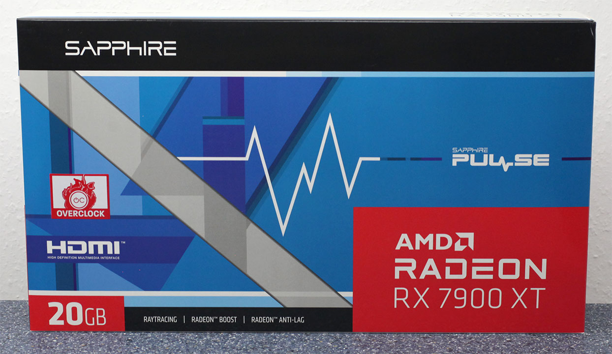
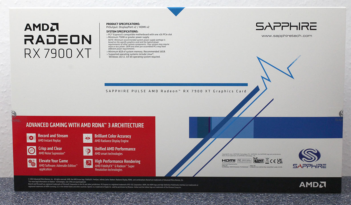
Packaging
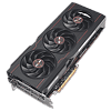
The Card
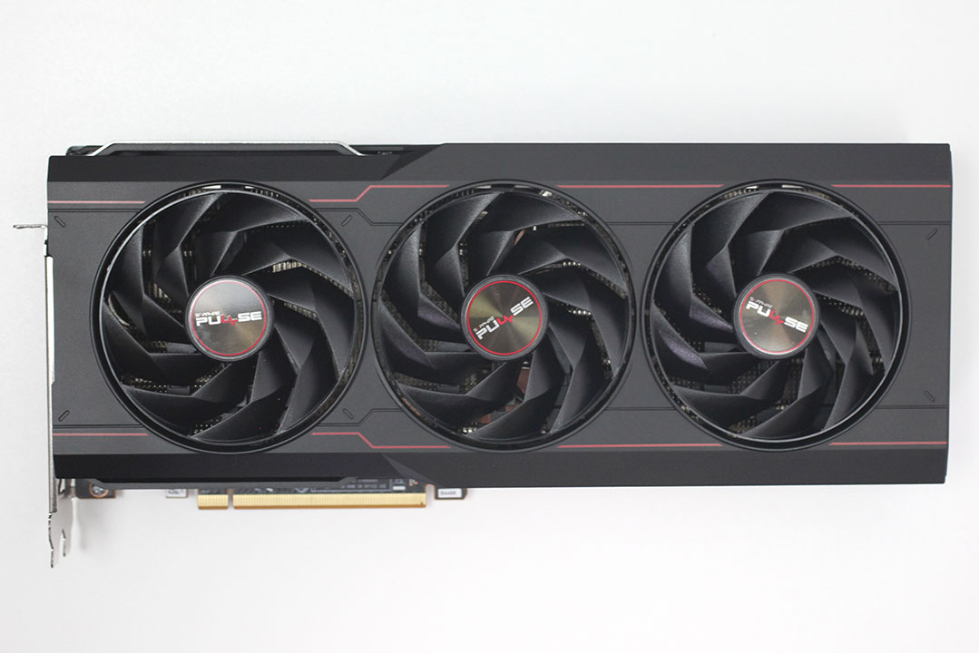
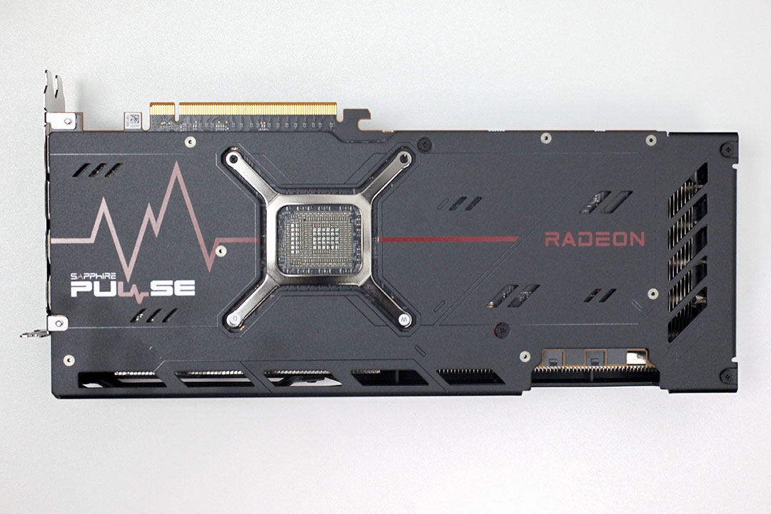
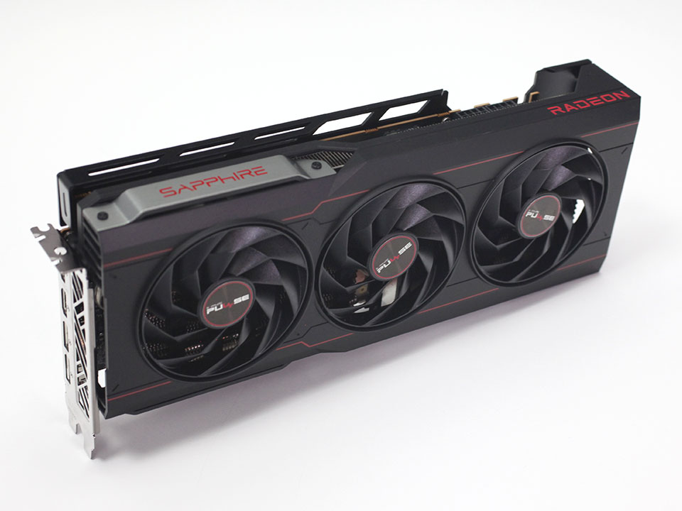
Sapphire Pulse design for the RX 7900 Series follows the design theme of the previous generation—black is the dominant color with red highlights. On the back, you'll find a metal backplate, which is designed to let some airflow through the cooler.
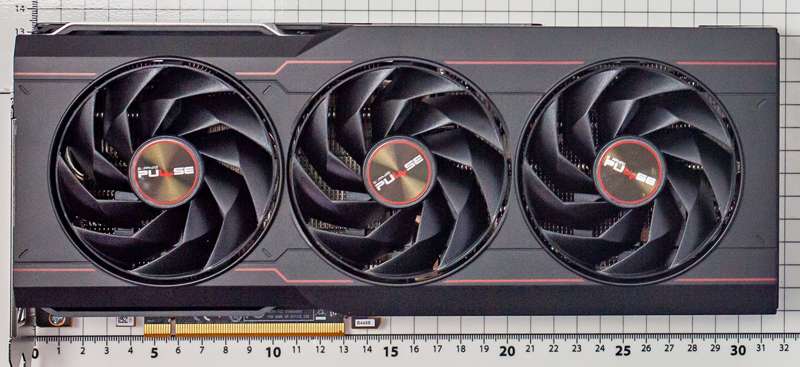

Dimensions of the card are 31.5 x 13.5 cm, and it weighs 1420 g.

Installation requires three slots in your system.
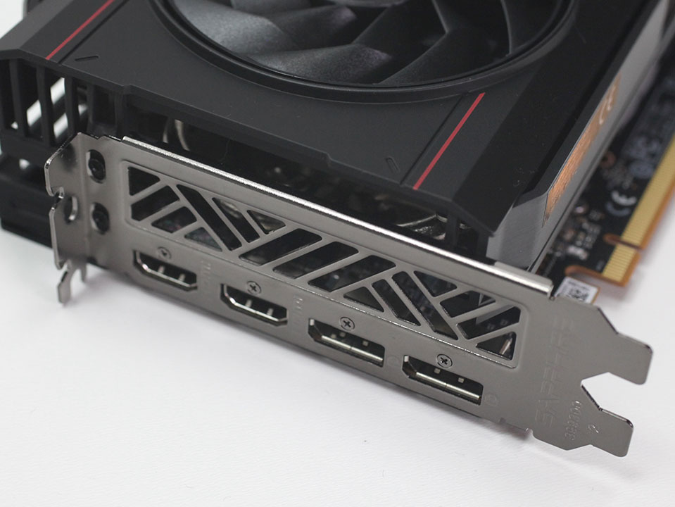
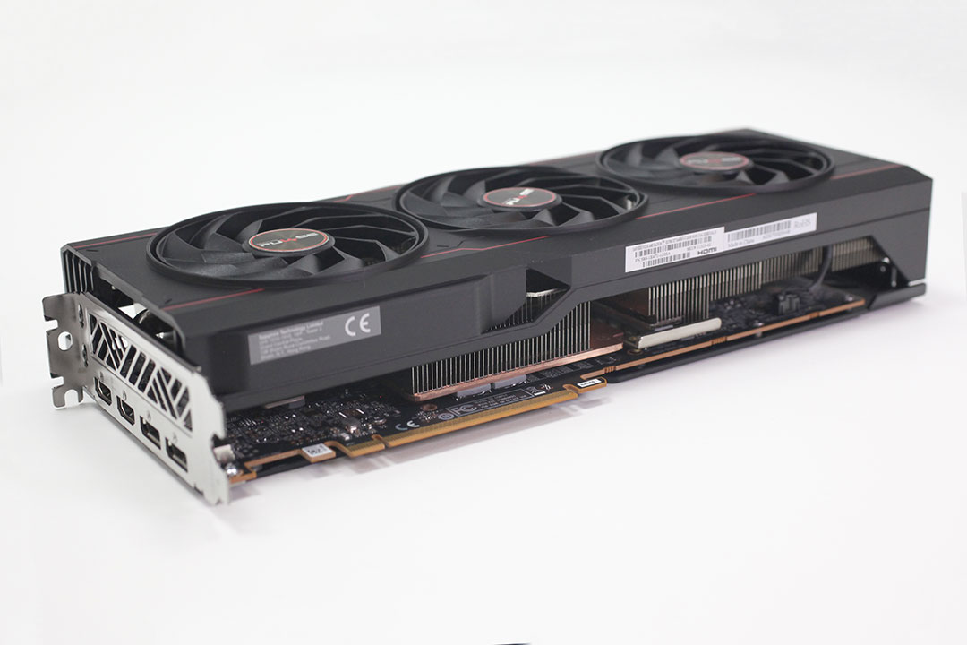
Display connectivity includes two standard DisplayPort 2.1 ports (RDNA2 had 1.4a) and two HDMI 2.1a (same as RDNA2).
AMD has upgraded their encode/decode setup. It now comes with two independent hardware units that can encode and decode two streams of video in parallel, or one stream at double the FPS rate. There's support for VP9, H.264, H.265 and AV1 decode, and encoding is supported for H.264, H.265 and AV1.
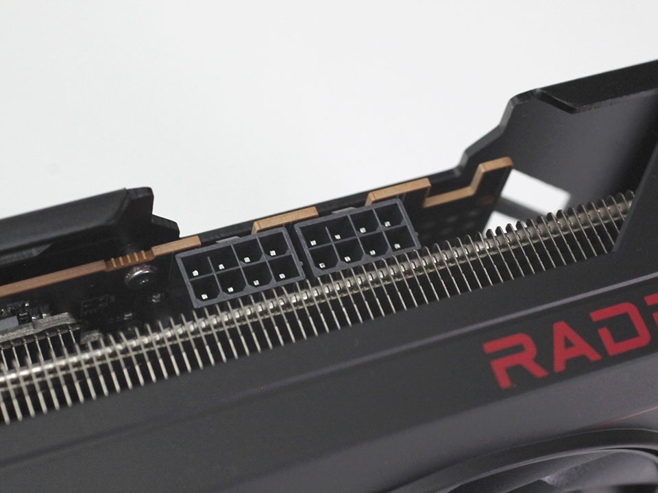
The card uses a classic dual 8-pin power input config, rated for 375 W maximum power. NVIDIA on the other hand uses the new 12+4 pin ATX 12VHPWR connector, which is rated for up to 600 W of power draw.
Teardown

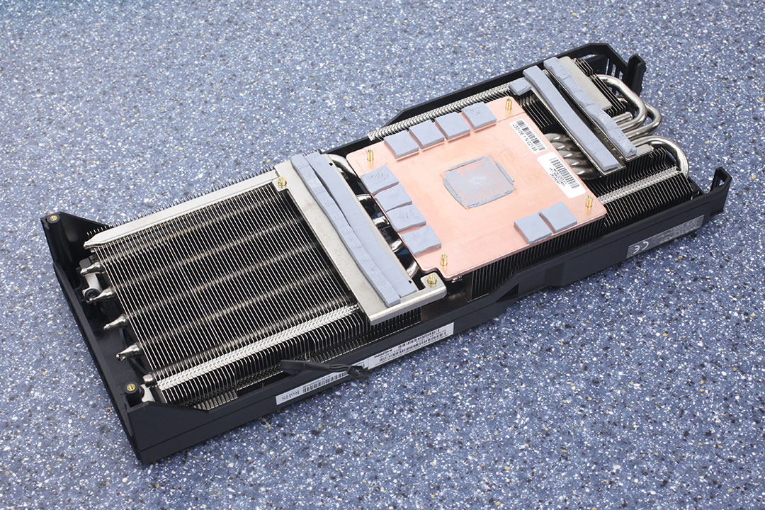
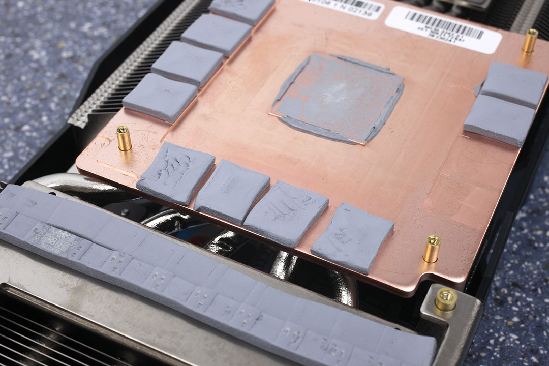
Sapphire's thermal solution provides cooling not only for the GPU, but also the memory chips and voltage regulator circuitry. There's five heatpipes on the cooler.
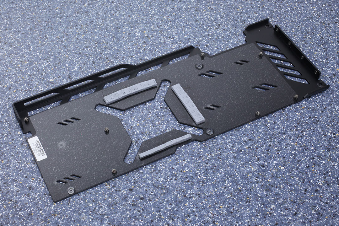

The backplate is made of metal and protects the card against damage during installation and handling.
High-resolution PCB Pictures
These pictures are for the convenience of volt modders and people who would like to see all the finer details on the PCB. Feel free to link back to us and use these in your articles, videos or forum posts.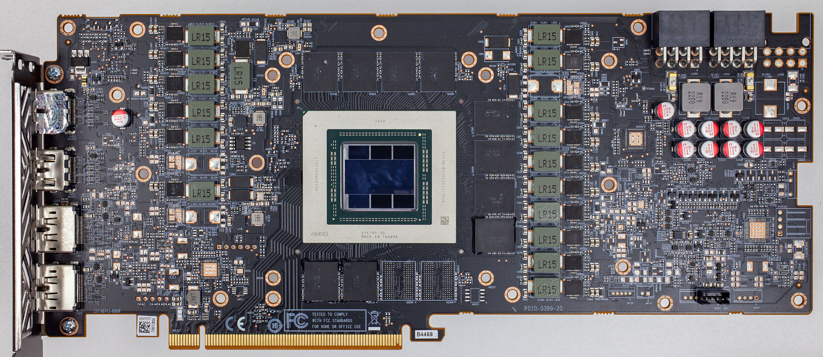
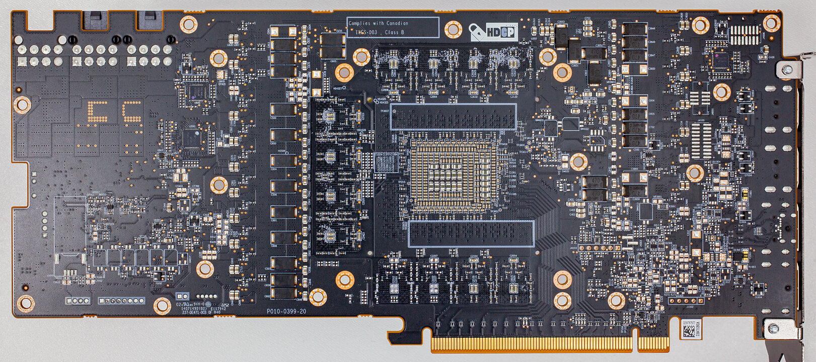
High-resolution versions are also available (front, back).
Circuit Board (PCB) Analysis
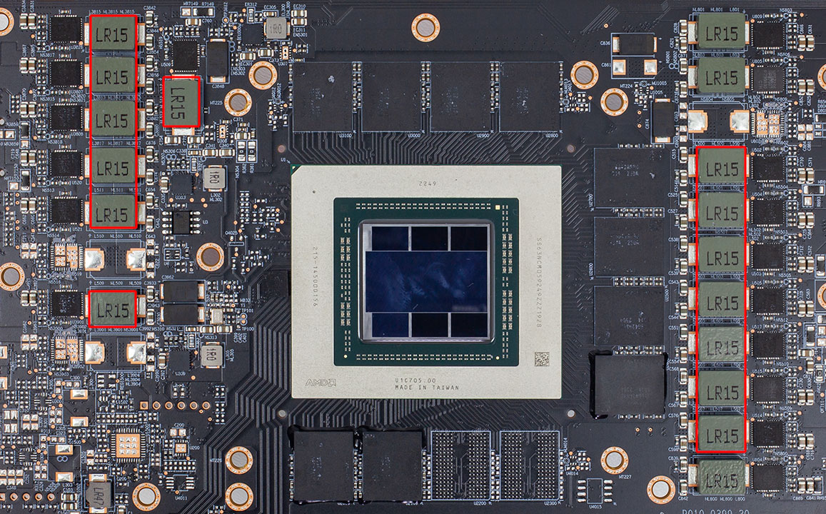
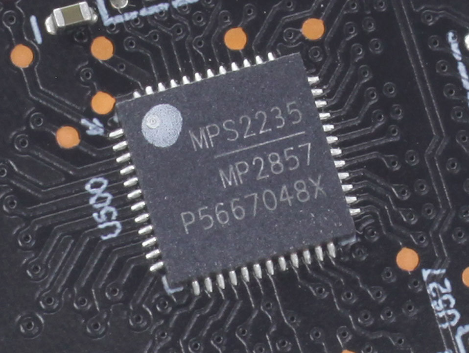
GPU voltage is a 14-phase design, managed by a Monolithic Power Systems MP2857 controller.

Monolithic MP87997 DrMOS components are used for GPU voltage; they are rated for 70 A of current each.
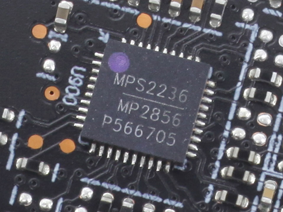
Memory voltage is a three-phase design, managed by a Monolithic Power Systems MP2856 controller.
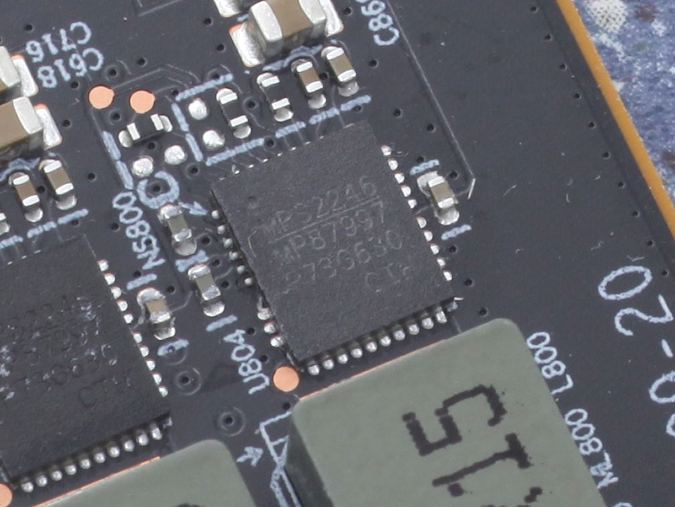
For memory, Monolithic MP87997 DrMOS with a 70 A rating are used again.
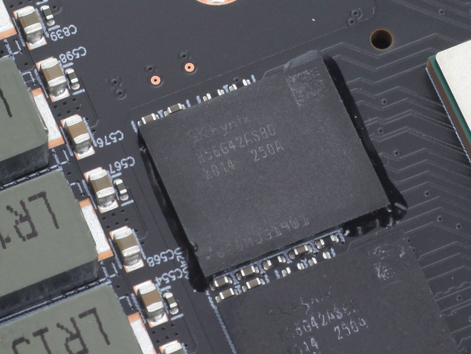
The GDDR6 memory chips are made by Hynix and carry the model number H56G42AS8DX-014. They are specified to run at 2500 MHz (20 Gbps effective).

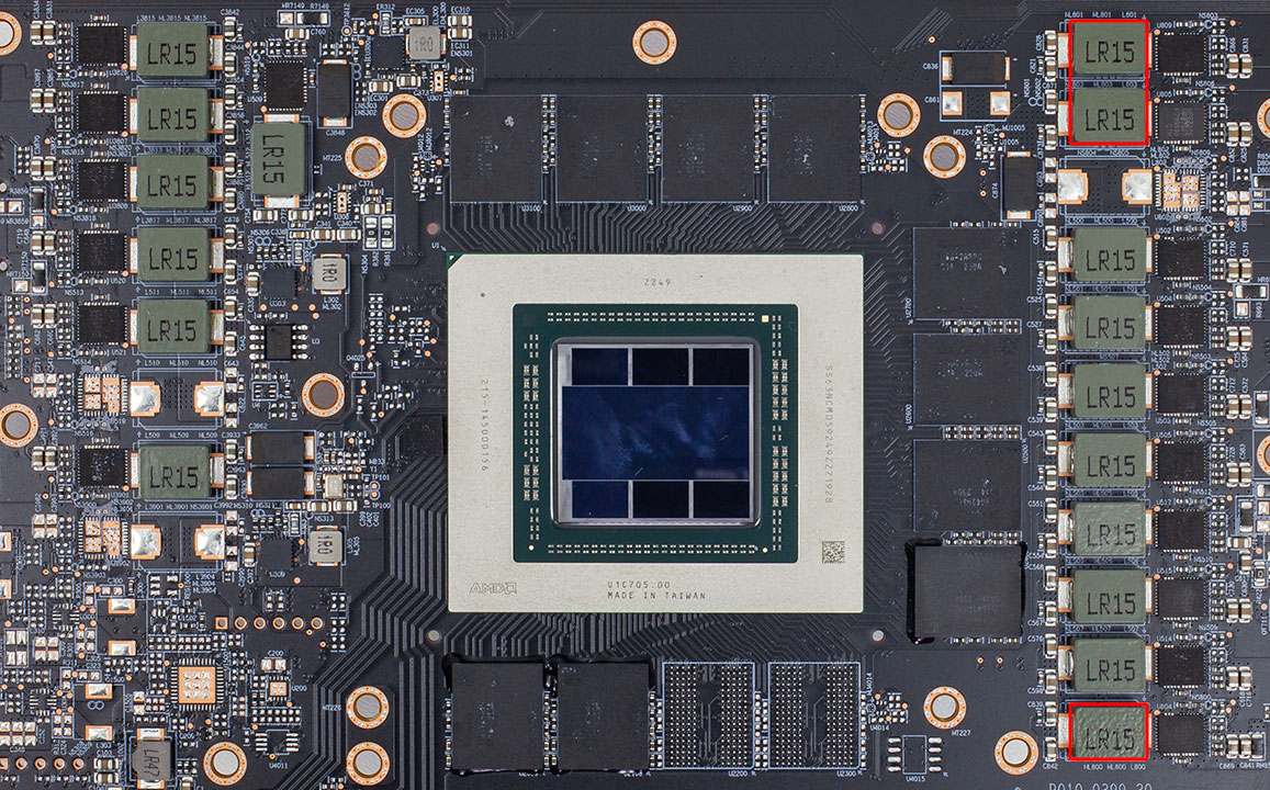
AMD's Navi 31 graphics processor is the world's first GPU that uses a chiplet architecture. Note the large die in the center, called "GCD," graphics compute die, which houses the compute units, it is surrounded by six smaller "MCD," memory cache dies, that contain one memory controller interface and one slice of cache each. While they look similar, the MCDs are not HBM chips. The MCDs are fabricated on a 6 nm process at TSMC Taiwan with a die size of 36.6 mm² each, the GCD is fabricated using TSMC's 5 nanometer node, with a die size of 300 mm². The combined transistor count of the GPU is 57.7 billion.
Our Patreon Silver Supporters can read articles in single-page format.
Apr 29th, 2024 13:21 EDT
change timezone
Latest GPU Drivers
New Forum Posts
- Why MS buying all of these Studios is bad for Gaming (51)
- What's your latest tech purchase? (20392)
- Is this Sapphire PULSE RX 5600 XT legit or fake? (0)
- Arctic MX-6 shelf life is just a couple months? (14)
- New High Performance, x86 Compatible Microprocessors from Centaur / VIA (146)
- PL1 | OMEN 17-cb0xxx / I7-9750H / RTX 2060 (4)
- Z790 ACE MAX? (5)
- Dialing in the overlock on my new 12600kf, matured silicon process showing great results... (17)
- Is it better for zero RPM PSUs to place the fan on top? (21)
- All I want is 2 monitors + 1 PC - Help! (2)
Popular Reviews
- Ugreen NASync DXP4800 Plus Review
- HYTE THICC Q60 240 mm AIO Review
- Upcoming Hardware Launches 2023 (Updated Feb 2024)
- MOONDROP x Crinacle DUSK In-Ear Monitors Review - The Last 5%
- Alienware Pro Wireless Gaming Keyboard Review
- FiiO K19 Desktop DAC/Headphone Amplifier Review
- Thermalright Phantom Spirit 120 EVO Review
- ASUS Radeon RX 7900 GRE TUF OC Review
- AMD Ryzen 7 7800X3D Review - The Best Gaming CPU
- Logitech G Pro X Superlight 2 Review - Updated with 4000 Hz Tested
Controversial News Posts
- Windows 11 Now Officially Adware as Microsoft Embeds Ads in the Start Menu (146)
- Intel Statement on Stability Issues: "Motherboard Makers to Blame" (140)
- Sony PlayStation 5 Pro Specifications Confirmed, Console Arrives Before Holidays (117)
- NVIDIA Points Intel Raptor Lake CPU Users to Get Help from Intel Amid System Instability Issues (106)
- AMD "Strix Halo" Zen 5 Mobile Processor Pictured: Chiplet-based, Uses 256-bit LPDDR5X (103)
- AMD's RDNA 4 GPUs Could Stick with 18 Gbps GDDR6 Memory (99)
- US Government Wants Nuclear Plants to Offload AI Data Center Expansion (98)
- TechPowerUp Hiring: Reviewers Wanted for Motherboards, Laptops, Gaming Handhelds and Prebuilt Desktops (89)