 35
35
Sparkle Arc A580 Orc Review
Pictures & Teardown »Architecture
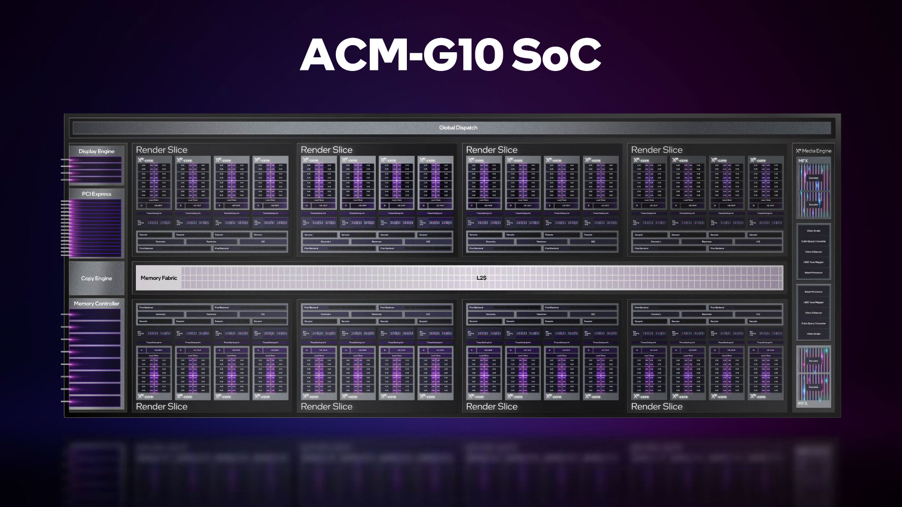
Intel Xe-HPG "Alchemist" graphics architecture sees its biggest implementation to date with the ACM-G10 silicon powering the A770, A750, and the new A580. Built on the 6 nm process at TSMC, the ACM-G10 measures 406 mm² in die-area, and packs 21.7 billion transistors. Much like NVIDIA and AMD, Intel has innovated its own hierarchy for the number-crunching machinery of its GPUs, and differentiates SKUs by changing the number of indivisible groups of these to meet performance targets. The ACM-G10 silicon features a PCI-Express 4.0 x16 host interface, a 256-bit wide GDDR6 memory interface, the Xe Media Engine and Xe Display Engine, among a global dispatch processor, and memory fabric that's cushioned by L2 cache. The main SIMD component top-level organization is the Render Slice. Each of these is a self-contained unit with all the number-crunching and raster graphics hardware a GPU needs.


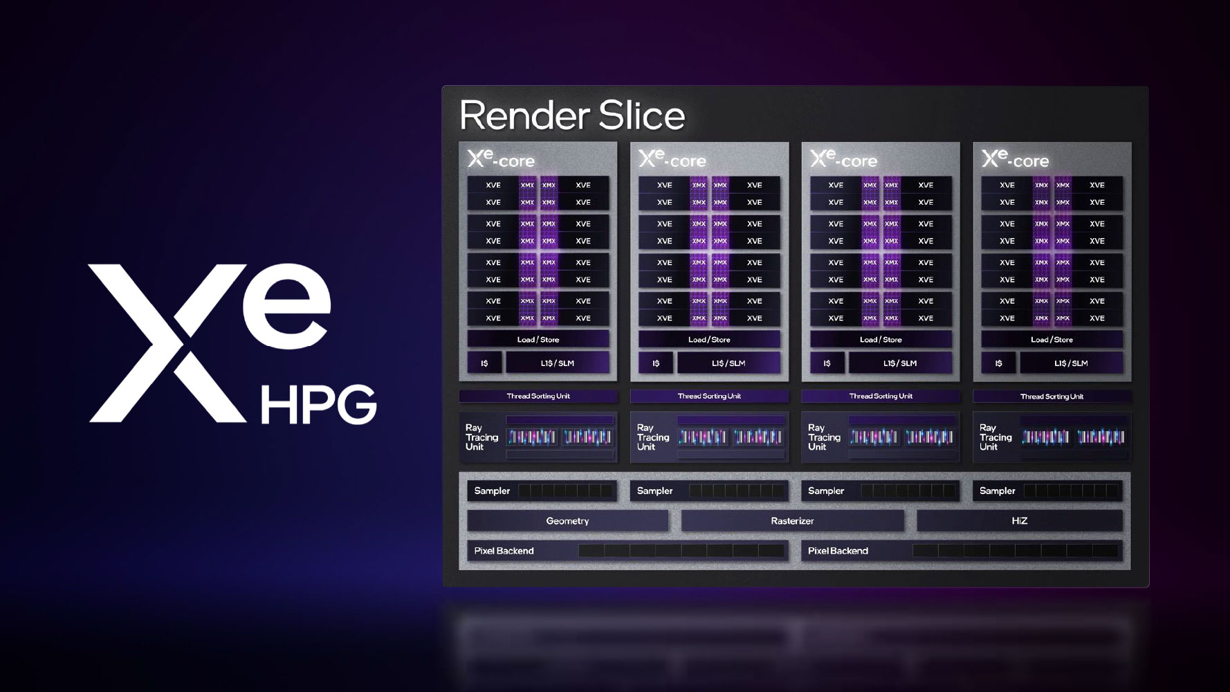
The ACM-G10 features eight such Render Slices. Each of these features four blocks of indivisible processing machinery, called Xe Cores; four Ray Tracing Units (RT units), and DirectX 12 Ultimate optimized raster-graphics units that includes four Samplers, Tessellation geometry processors, 16 ROPs, and 32 TMUs. Since there are 8 Render Slices, the silicon physically has 16 RT units, 128 ROPs, and 256 TMUs.


The Xe Core is the indivisible computation core, with sixteen 256-bit Vector Engines (execution units), sixteen 1024-bit XMX Matrix Engines, and 192 KB of L1 cache. Each Vector Engine has eight each of FP and INT units, besides a register file. Two adjacent Vector Engines share a Thread Control unit to share execution waves. There are 16 VEs per Xe Core, 4 Xe Cores per Render Slice, and 8 Render Slices on the ACM-G10 silicon, so we have 512 execution units in all, each with 8 FP/INT execution stages, which logically work out to 4,096 unified shaders. The A580 is carved out of this silicon by leaving the memory sub-system untouched, but enabling just 24 out of 32 Xe cores, by disabling two Render Slices. This results in 384 execution units, or 3,072 unified shaders, 384 XMX cores for AI acceleration, 24 Ray Tracing Engines, 192 TMUs, and 96 ROPs.
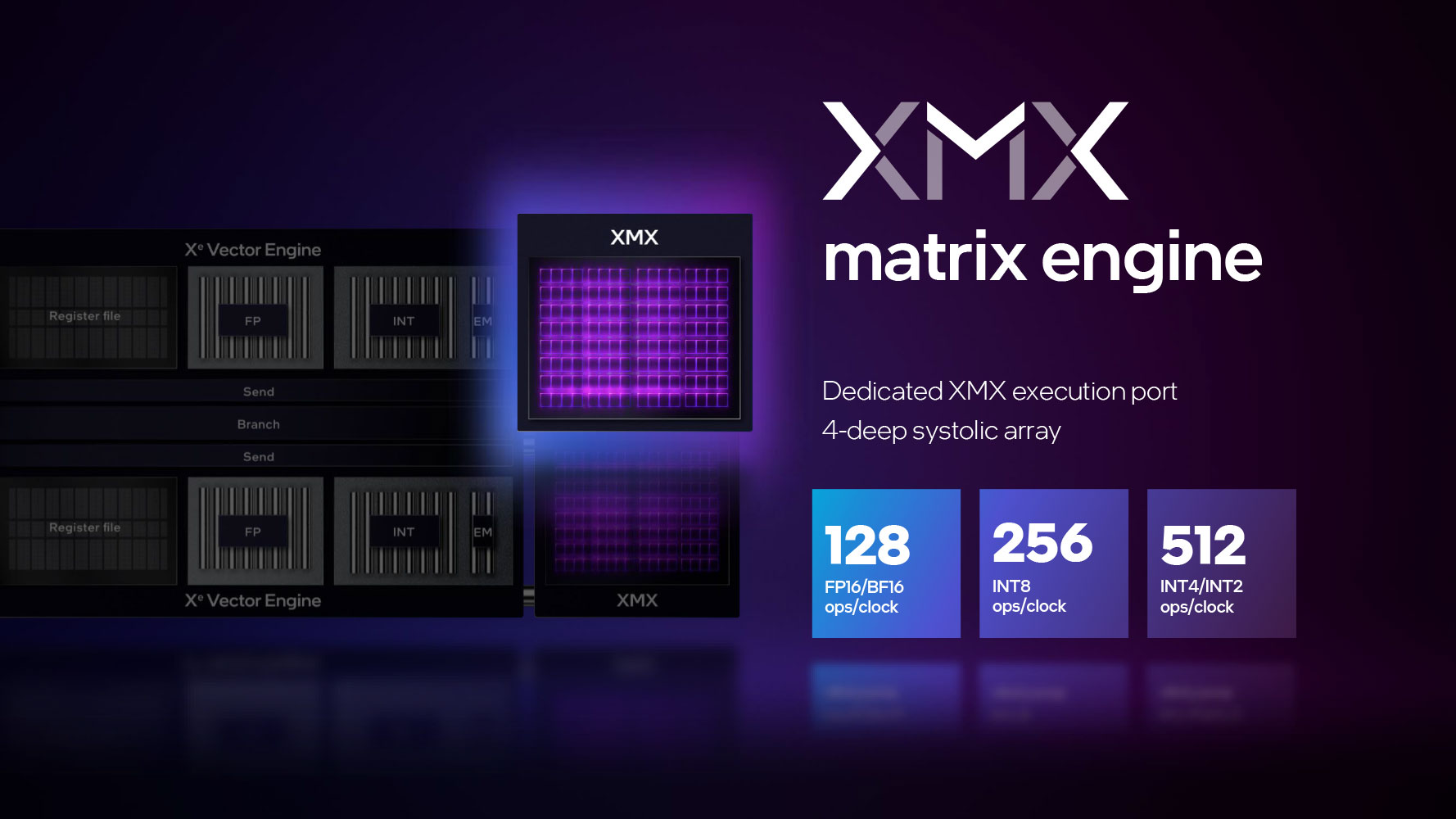

The XMX Matrix Engine is an extremely capable matrix-multiplication fixed-function hardware that can accelerate AI deep-learning neural net building and training. It's also a highly capable math accelerator. Intel originally designed this technology for the Xe-HP AI processors, but it finds client applications in Arc Graphics, where it is leveraged for ray tracing denoising and to accelerate features such as XeSS. There are 16 XMX units per Xe Core, and 64 per Render Slice, 512 across the ACM-G10 silicon. Each XMX unit can handle 128 FP16 or BF16 operations per clock; up to 256 INT8 ops/clock, and 512 INT4 ops/clock. The XMX-optimized native XeSS code is an order of magnitude faster than the industry-standard DP4a codepath of XeSS, as you'll see in our testing.
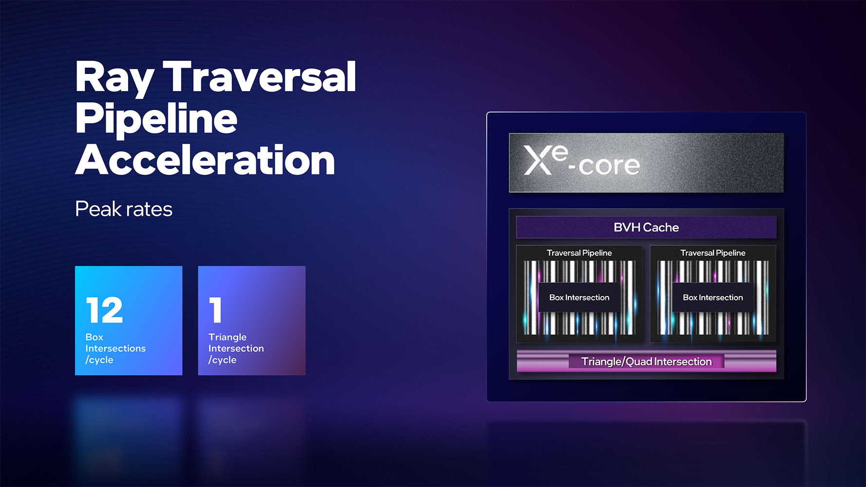
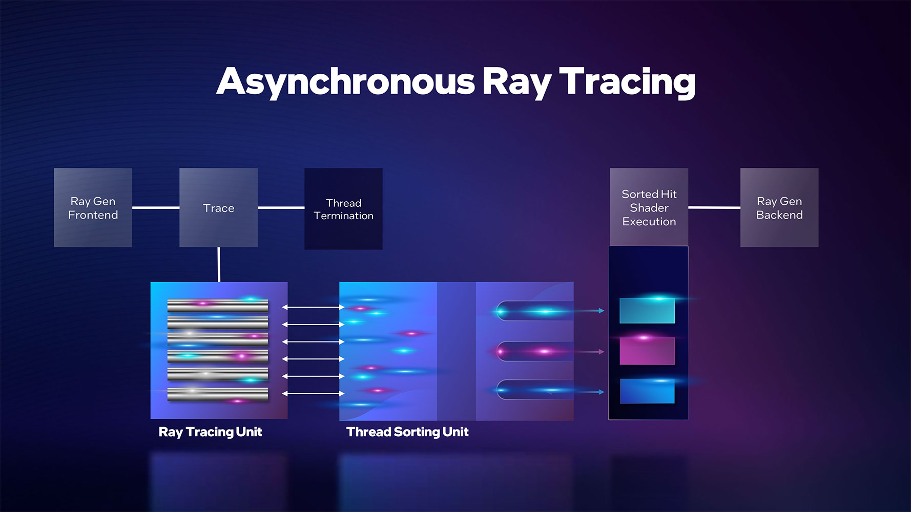
When it comes to real time ray tracing, Intel's Xe-HPG architecture has technological-parity with NVIDIA RTX, due to its heavy reliance on fixed-function hardware for ray intersection, BVH, and AI-based denoising.

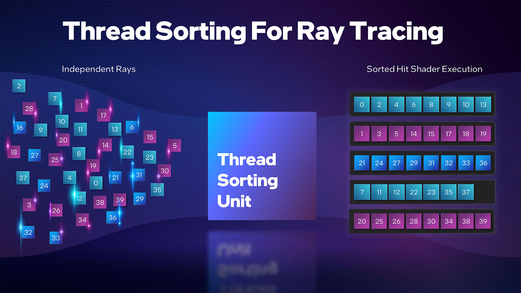
There are several optimizations that further reduce the burden of ray tracing operations on the main SIMD machinery, such as shader execution reordering which optimizes shader work threads for streamlined execution among the SIMD units. NVIDIA is only now implementing such a feature, with its GeForce "Ada" architecture. There's a special component in each Xe Core that reorders shader threads. It's essentially a very intelligent dispatch unit. Intel refers to its ray tracing architecture as Asynchronous.


With Moore's Law tapering despite Intel claiming otherwise, the writing is on the wall—rendering at native resolution is over, at least in the performance and mainstream GPU segments. High-quality super resolution features such as DLSS and FSR are helping NVIDIA and AMD shore up performance at minimal quality loss, by rendering games at lower resolutions than native to the display; and upscaling them intelligently, with minimal quality losses. Intel's take is XeSS. The company claims that this is a 2nd generation super-res technology, on par with DLSS 2 and FSR 2.0. The XeSS upscaling tech is as easily integrated with a game engine's rendering pipeline as TAA (or AMD FSR). The XeSS algorithm is executed as XMX-optimized AI on Arc GPUs, and as DP4a-compatible code on other GPU brands. The algorithm takes into account low-resolution frame data, motion vectors, and temporal data from previously output high-res frames to reconstruct details, before passing on the high-res output to the game engine for post-processing and UI/HUD.
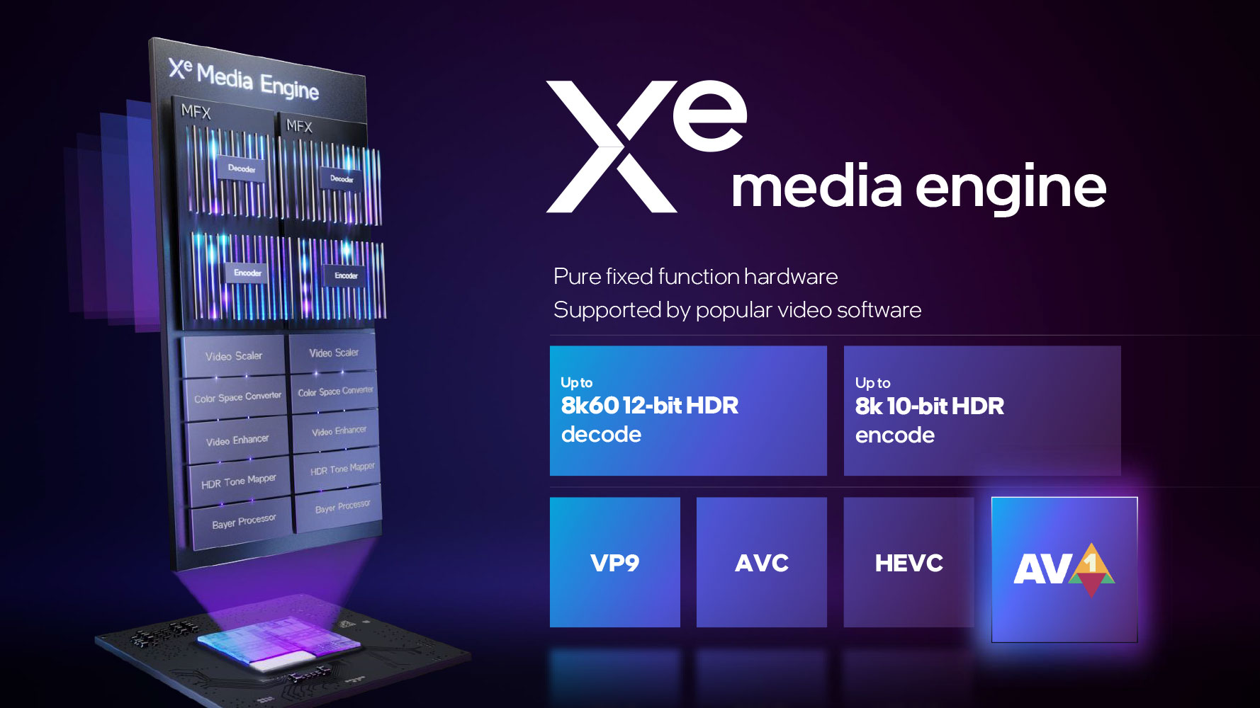
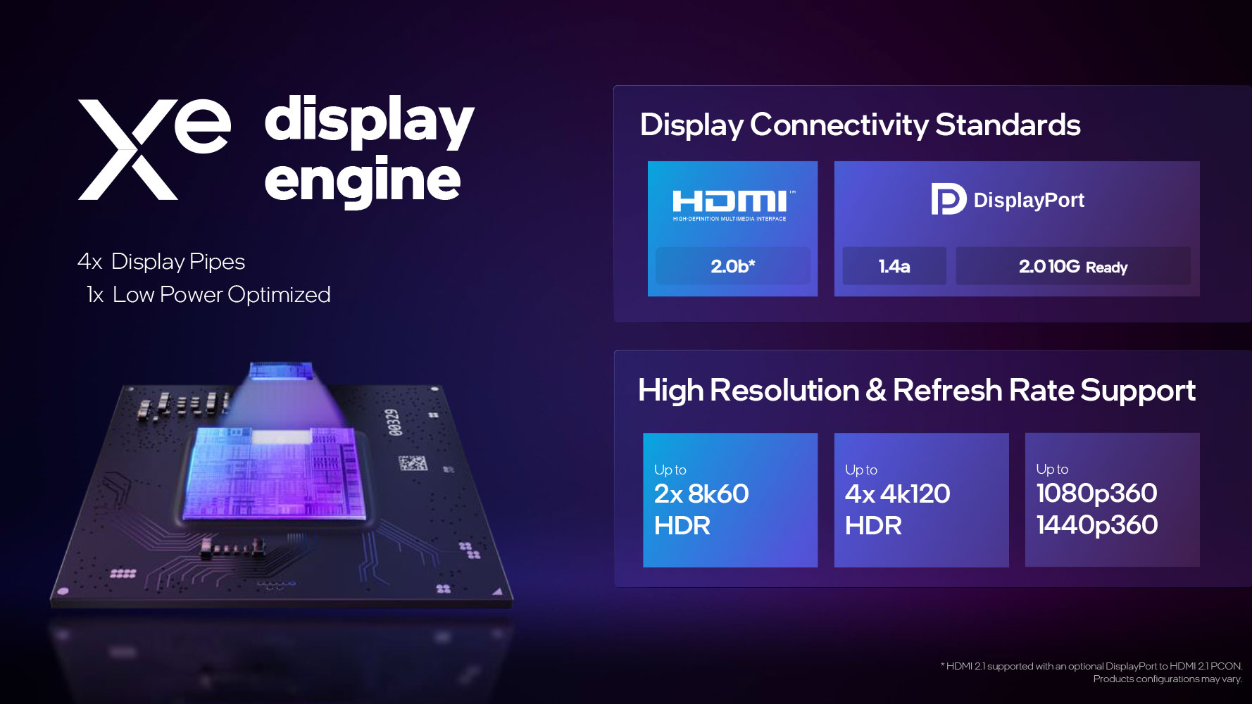
The Xe Display Engine is capable of up to two display outputs at 8K 60 Hz + HDR; up to four outputs at 4K 120 Hz + HDR, and up to four 1440p or 1080p with 360 Hz + HDR. VESA Adaptive Sync and Intel Smooth Sync features are supported. The latter is a feature that runs the GPU at its native frame-rate, while attempting to remove the screen-tearing from the display output. A typical Arc desktop graphics card has two each of DisplayPort 2.0 and HDMI 2.0b connections. The Xe Media Engine provides hardware-accelerated decoding and encoding of AV1, and accelerated decoding of H.265 HEVC, and H.264 AVC.

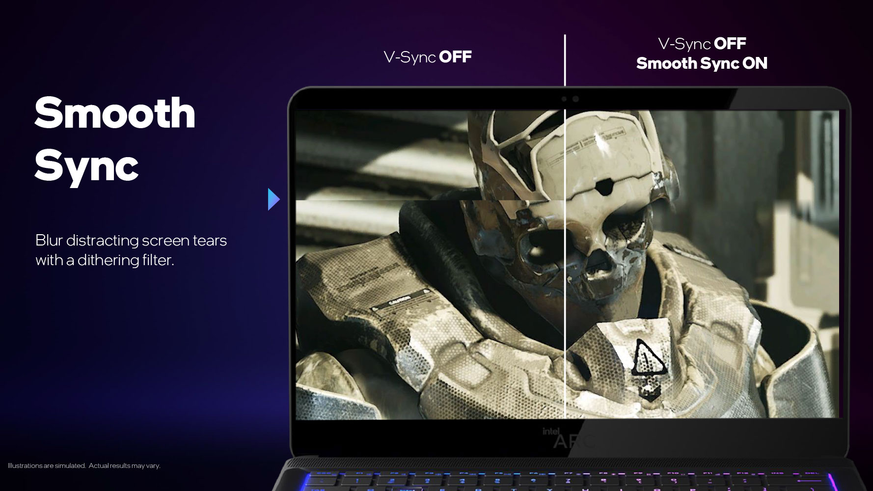
Besides VESA Adaptive Sync, the Xe Display Engine offers a software feature called Smooth Sync. This gives fixed refresh-rate monitors the ability to play games without V-Sync, rendering them at the highest possible FPS (and the least input latency), while attempting to eliminate the screen-tearing using a shader-based dithering filter pass. This is an extremely simply way to solve this problem, and we're surprised AMD and NVIDIA haven't tried it.
May 12th, 2024 17:50 EDT
change timezone
Latest GPU Drivers
New Forum Posts
- Alphacool 280 xt45 Radiator repair (12)
- Which Audio System Would you Choose and Why? (5)
- Air makes its way from the reservoir into the radiator. (37)
- Purchased an AX1200i PSU as part of some forward planning, what tier is this PSU? (55)
- Regular frametime spikes in all games (8)
- LOL ASUS says this is $200 in repair, Steve from gamers Nexus smokes ASUS, Steam Deck til I die boys!!!! (76)
- How to install nvidia driver for rtx3080 on windows 1709? (65)
- Xeon Owners Club (8703)
- How to optimize my PC by overclocking my system (5)
- I don't think Ryzen 9900x3d is just being announced next month, I think it's launching next month. (66)
Popular Reviews
- ZMF Caldera Closed Planar Magnetic Headphones Review
- ThundeRobot ML903 NearLink Review
- Corsair MP700 Pro SE 4 TB Review
- Bykski CPU-XPR-C-I CPU Water Block Review - Amazing Value!
- CHERRY XTRFY M64 Pro Review
- Upcoming Hardware Launches 2023 (Updated Feb 2024)
- ASRock NUC BOX-155H (Intel Core Ultra 7 155H) Review
- AMD Ryzen 7 7800X3D Review - The Best Gaming CPU
- Corsair iCUE Link RX120 RGB 120 mm Fan Review
- ASUS Radeon RX 7900 GRE TUF OC Review
Controversial News Posts
- Intel Statement on Stability Issues: "Motherboard Makers to Blame" (266)
- AMD to Redesign Ray Tracing Hardware on RDNA 4 (219)
- Windows 11 Now Officially Adware as Microsoft Embeds Ads in the Start Menu (171)
- NVIDIA to Only Launch the Flagship GeForce RTX 5090 in 2024, Rest of the Series in 2025 (147)
- Sony PlayStation 5 Pro Specifications Confirmed, Console Arrives Before Holidays (119)
- AMD's RDNA 4 GPUs Could Stick with 18 Gbps GDDR6 Memory (114)
- AMD Hits Highest-Ever x86 CPU Market Share in Q1 2024 Across Desktop and Server (108)
- AMD Ryzen 9 7900X3D Now at a Mouth-watering $329 (104)