 12
Thermaltake Dockpower FI 1000W Review
Test Methodology »Internals


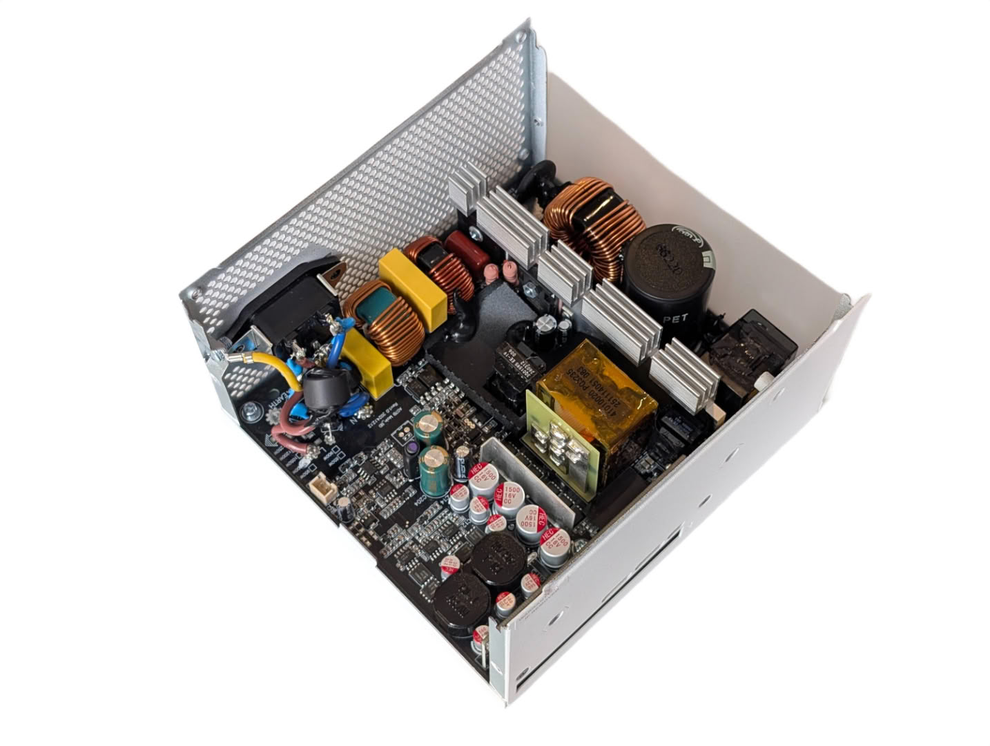
Taking a look inside, we see a somewhat familiar layout, with some aspects the same as in the Formula V Line FV and Moiplay Ora Pro G1 platforms. The general layout is exactly the same, especially around the minor rails DC-DC converter, 12 V transformer style, and control ICs hidden under the same plastic shroud. It isn't the same PCB, but it's heavily based on the same design.
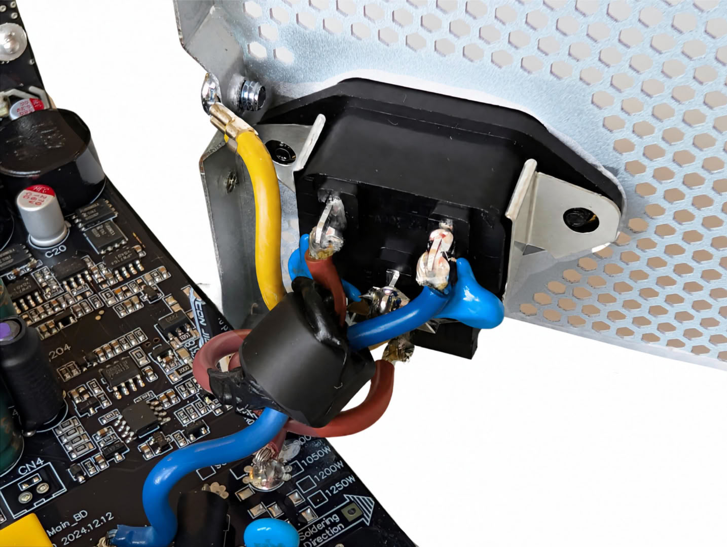


The power connector is loaded with a pair of Y caps, and a ferrite ring around the mains cables to reject HF noise. On the main board there is another pair of Y caps, MOV and fuse, and our first X cap. A little further down there is a CM choke followed by a second X cap and Y cap hiding underneath.
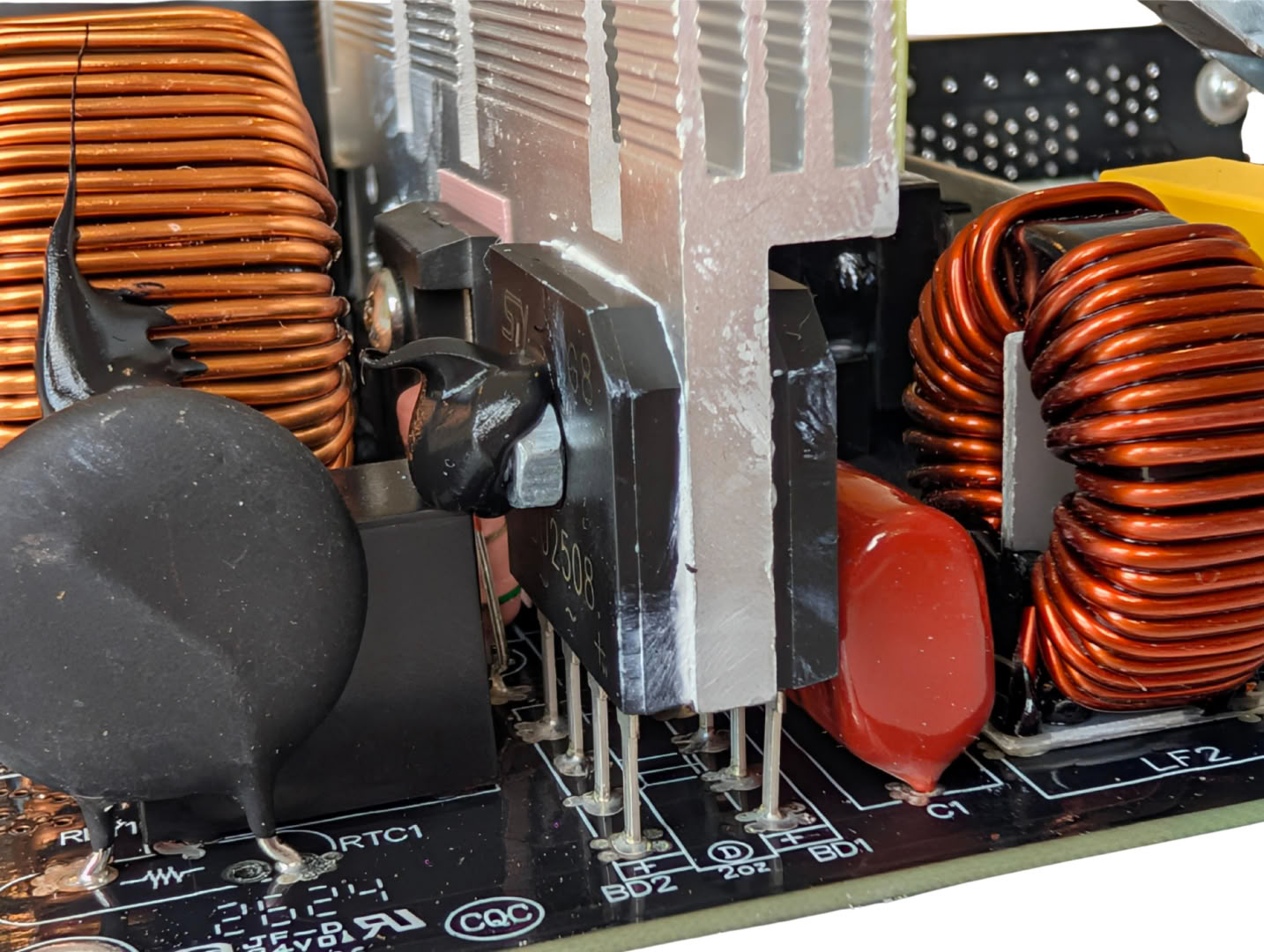
Rectifying the main AC is this pair of full bridge rectifiers, sharing a heatsink with some of the PFC components.
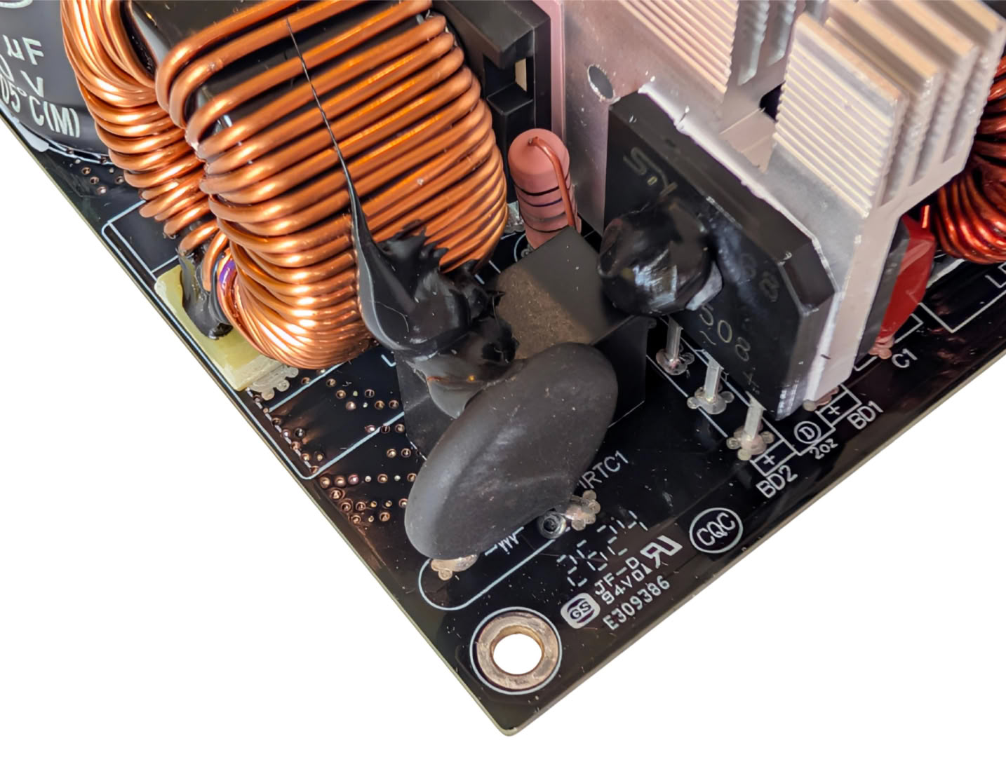
Inrush suppression is handled after rectification by this thermistor, bypassed by the relay once the bulk cap is sufficiently charged.
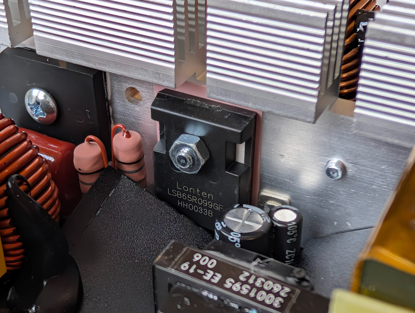
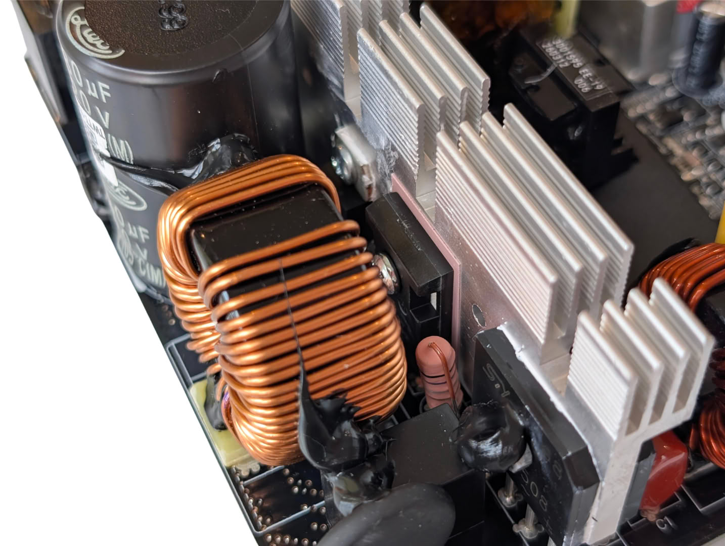
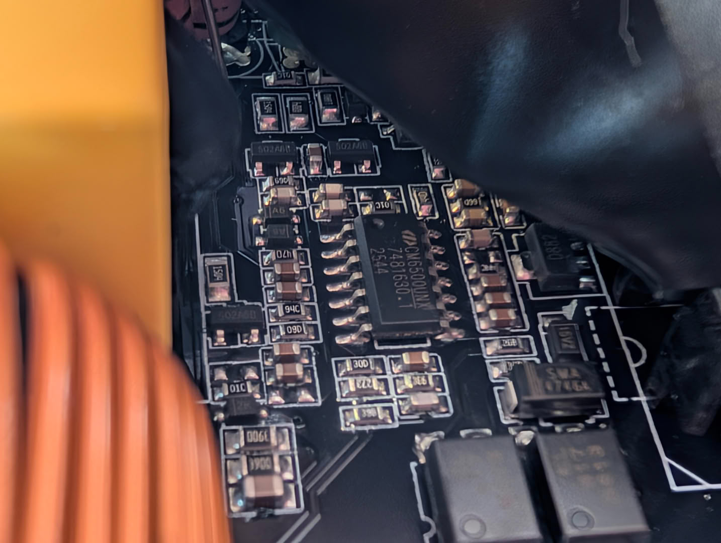
Active PFC is handled by a CM6500UNX IC. This is a single PFC controller specifically designed for increasing efficiency over previous PFC integrations, with a maximum speed of 1 MHz, and features zero-voltage switching behavior to boost lower load efficiency. It can drive semiconductor gates directly. The discrete components share a heatsink with the main rectifiers, just in front of the PFC inductor.
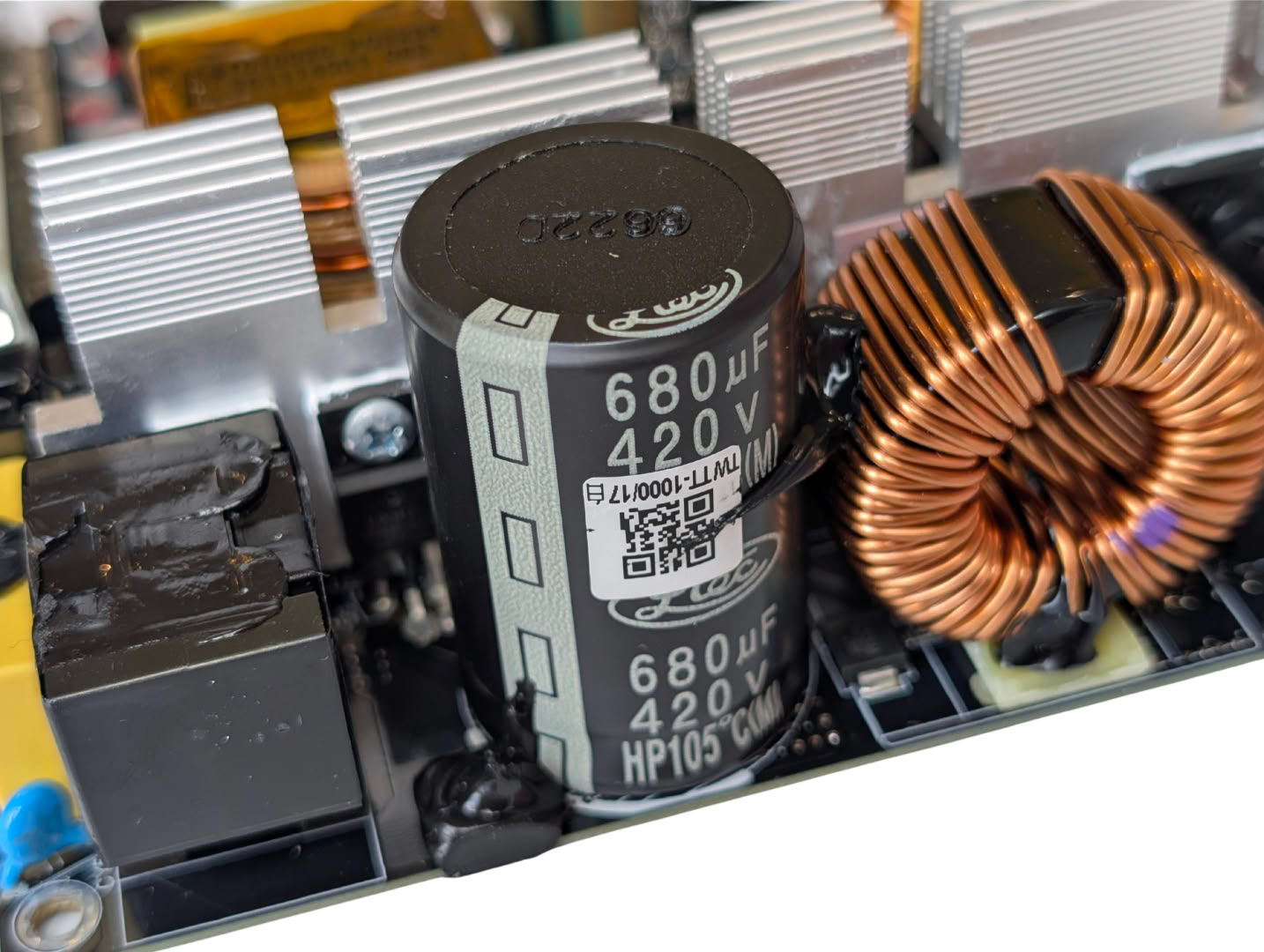
The features of the CM6500UNX allow for less bulk capacitance to be used, and so we find a single 420 V 680 uF LTEC 105°C HP model, which is their standard snap-in terminal line.
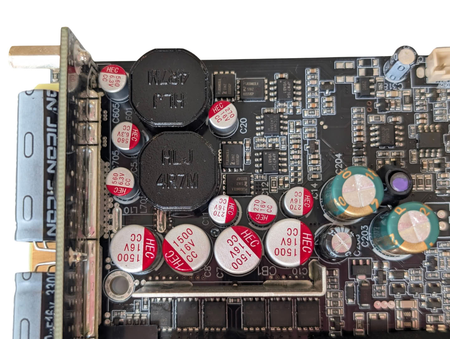
The four MOSFETs generating the auxiliary rails are PTJ030N03LA, seen in a plethora of PSUs in recent years. The inductors are seated flat to the board and completely encased, unlike the aforementioned models sharing similar PCBs, which have open upright inductors in this same location.
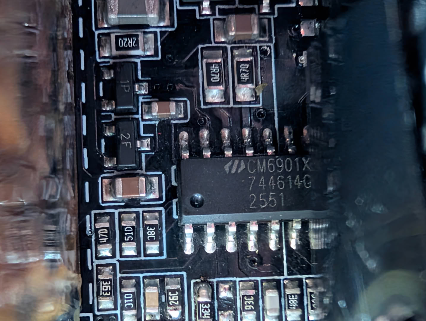
The main resonant controller is the CM6901, hiding under a plastic cover. This appears to be mainly handling the DC-DC conversion at the main 12 V rail since APFC is already taken care of by the CM6500.
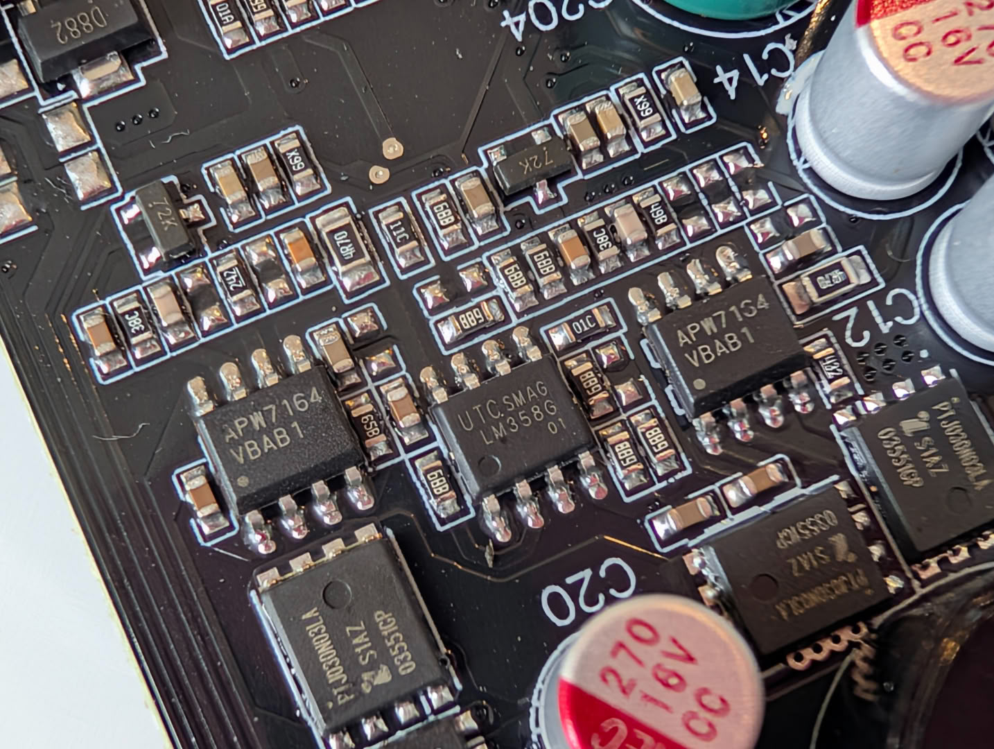
Soldering quality looks consistent and of perfectly adequate quality.
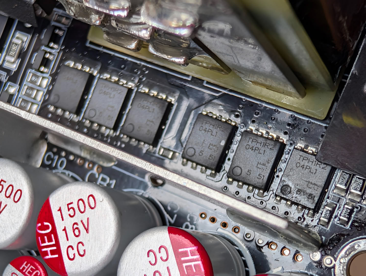
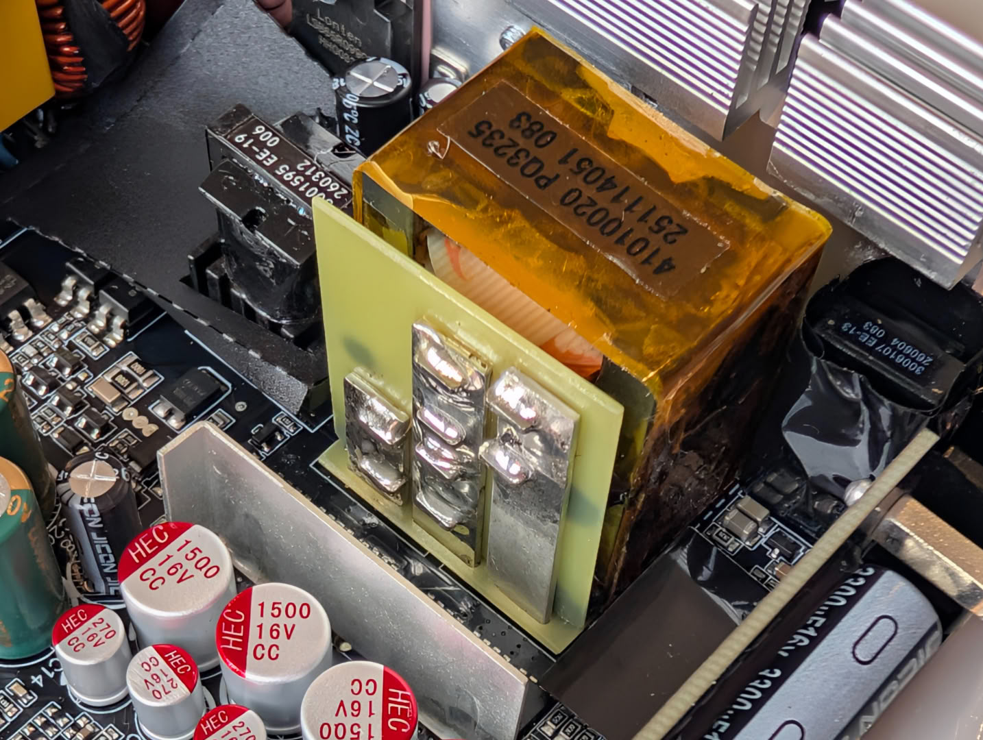
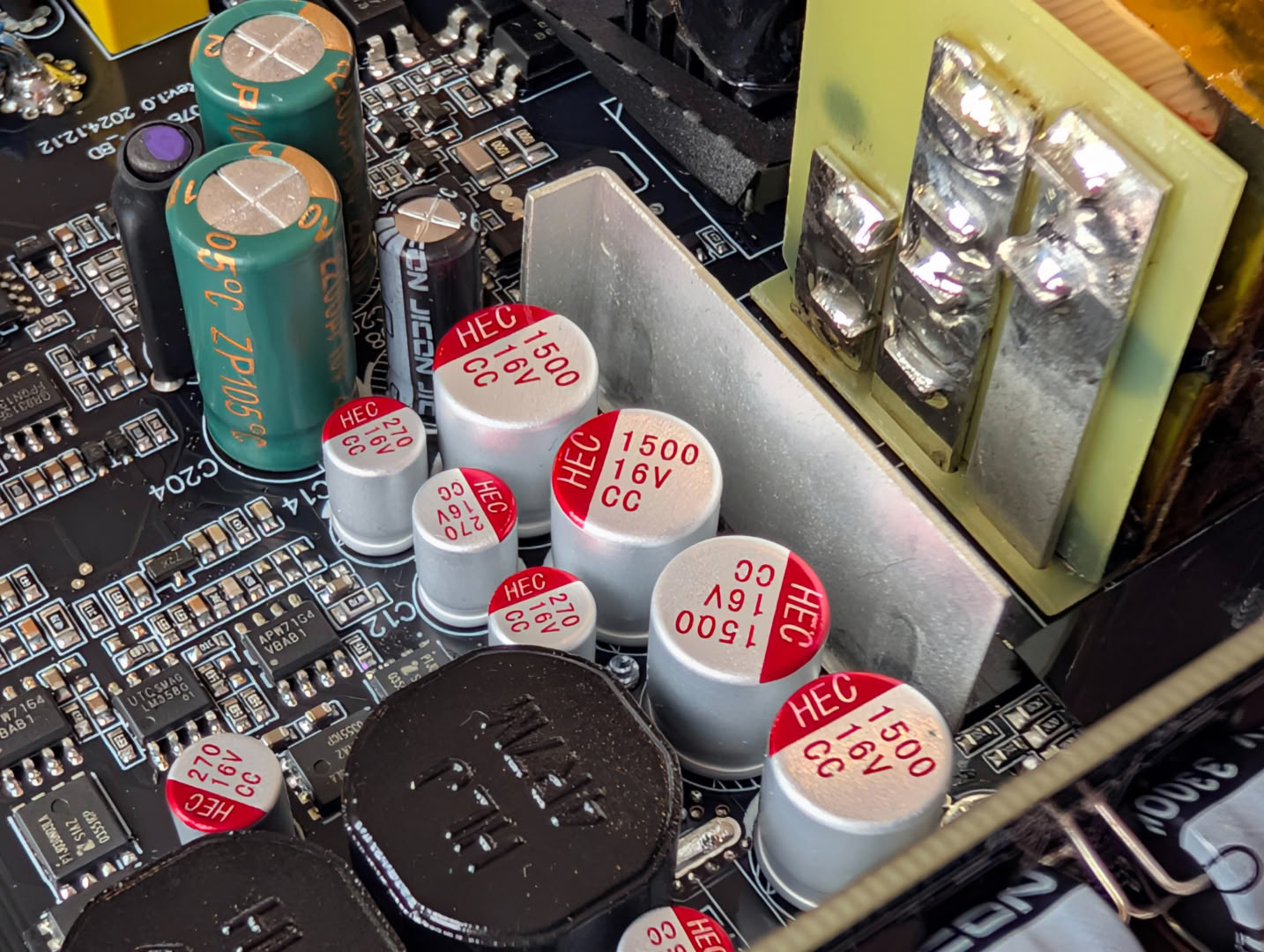
Driving the 12 V rail are six Toshiba TPH1R204PL1 MOSFETs, which are rated for 40 V, 270 A and have an RDS(on) of just 1.0 mΩ, allowing for extremely cool operation and minimal required heatsink capacity. Atop the PCB there is only a small metal bar acting as surface area for heat to escape. The transformer is set on its side, potentially to save space, and uses single core flat wire.
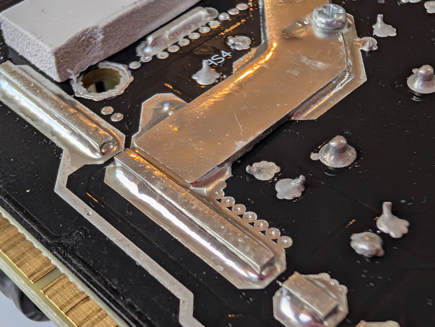
In addition to the bar, there is a plate acting as thermal mass under the 12 V MOSFETs, and a thick thermal pad which will couple the PCB to the main chassis to soak further heat.
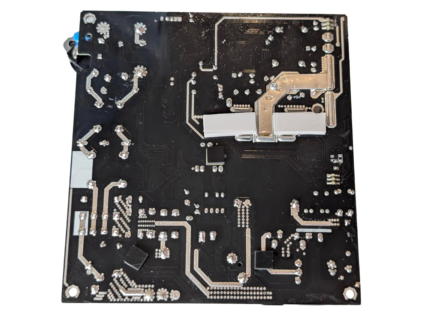
The underside of the PCB is devoid of active components, allowing for maximum trace area and ideal routing for all the main current-carrying paths.
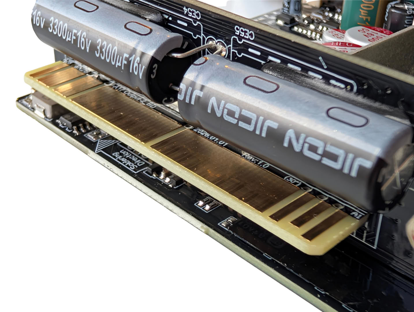
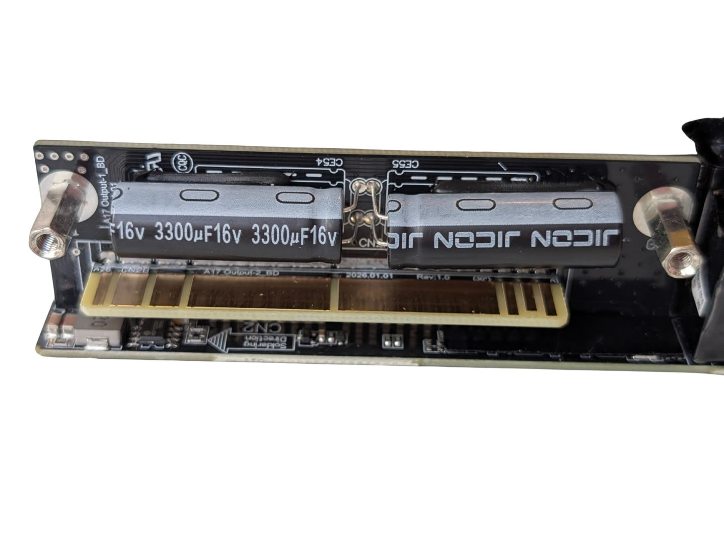
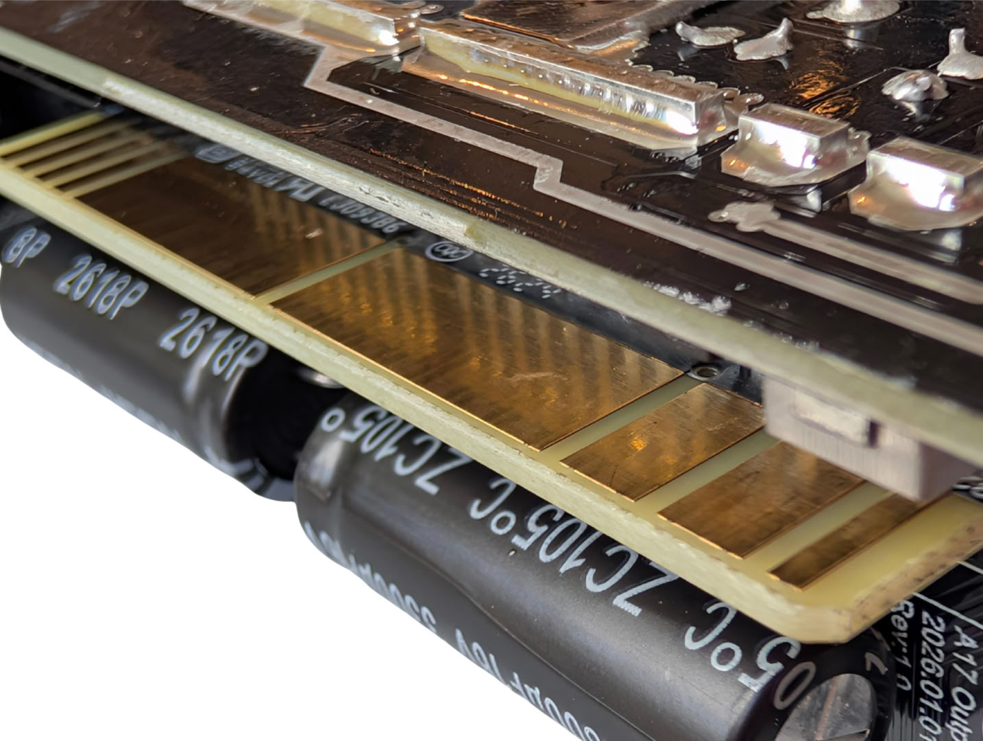
Here is a close look at the tab connecting the power rails to the dock. It consists of thick, wide gold-plated contacts on both the top and bottom of the tab. There are a pair of filter caps here also for the 12 V rail on this little upright board.
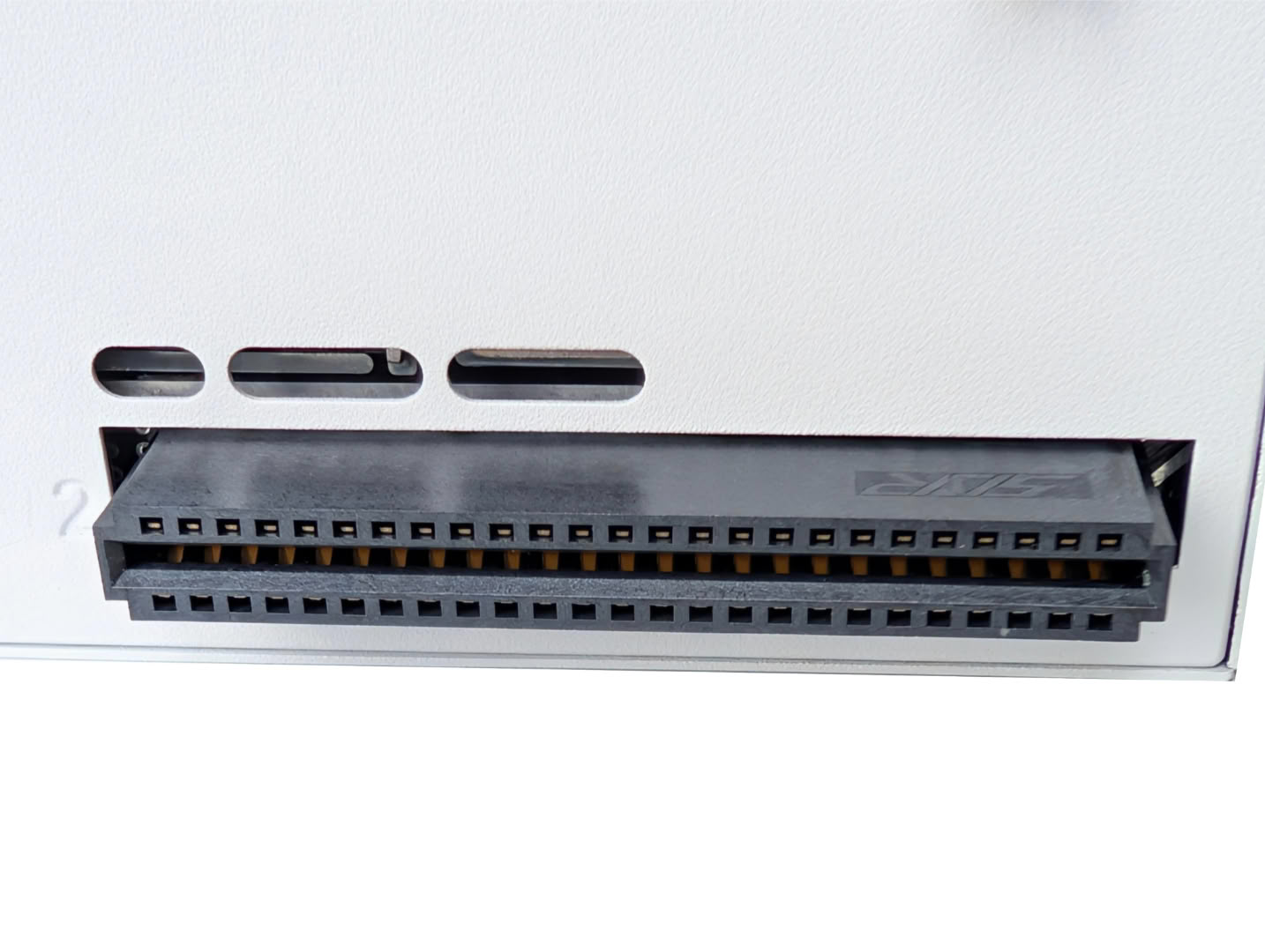
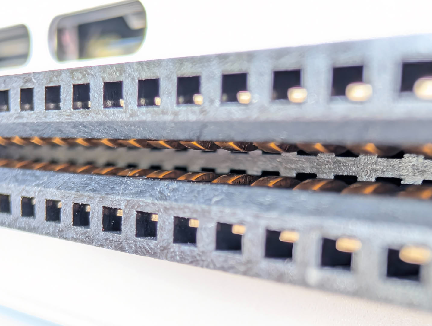
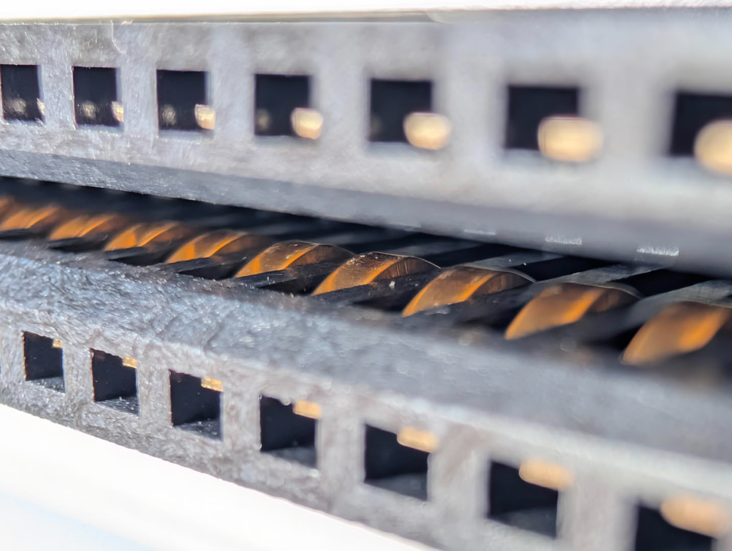
The dock-side connector mates up with individual gold-plated pins that apply reasonable clamping force to the tab. There will be a step-down in contact surface area from this, but it shouldn't be excessive, and we will test heat generated here later.
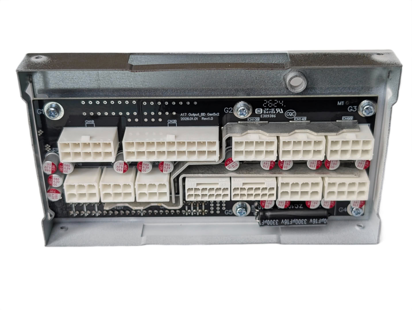
The dock itself simply houses the connector board usually integrated into the main body of a PSU. There are a few final filter caps by the connectors for all three power rails.
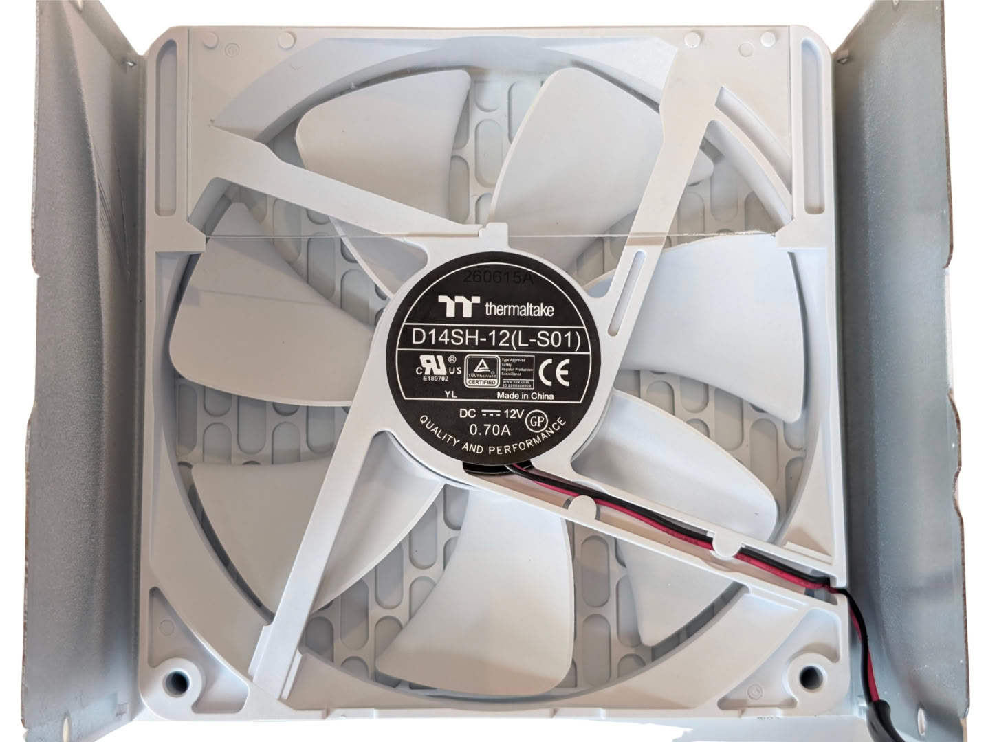
The fan used here is a variant specifically built for PSUs, so it should perform well. The aggressive blade design provides good static pressure and airflow even on de-tuned fan curves, since PSUs rarely allow a fan to run at full speed. There are some concerns about the lifespan of the sleeved bearing when mounted face-down in a power supply, as the oil moves down and the bearing runs dry, often causing mechanical noise, at higher speeds users will report noticeable hum and wind noise.
Nov 19th, 2026 15:34 CST
change timezone
Latest GPU Drivers
New Forum Posts
- Honestly, do you care about GTA VI? (163)
- Windows 11 General Discussion (7736)
- Current Sales, Bundles, Giveaways (10448)
- Last game you purchased? (1409)
- WarpCoreBench scores! (76)
- Got the EOL 32GB TridentZ 6000 CL26 1.4V (12)
- Dell Workstation Owners Club (3516)
- Making a game in Godot engine (4)
- DTS DCH Driver for Realtek HDA [DTS:X APO4 + DTS Interactive] (2815)
- Security Apps (2)
Popular Reviews
- Acemagic Retro X3 Review
- Ugreen NASync DXP4800 GT Review
- Upcoming Hardware Launches 2027 (Updated Nov 2026)
- Pulsar Office Tour & First Look at P1 Dual-Sensor Mouse
- AMD Zen 6 Technical Deep Dive
- Biwin Black Opal NV7400 2 TB Review
- Sapphire Radeon RX 7700 XT Pure Review
- Sapphire Radeon RX 7700 XT Pulse Review
- AMD Ryzen 7 9800X3D Review - The Best Gaming Processor
- Chieftec Iceberg PRO 360 DARK Review
TPU on YouTube
Controversial News Posts
- NVIDIA Co-Founder and CEO Jensen Huang Officially Resigns (487)
- Report: Jensen Huang Eyes NVIDIA Comeback (223)
- Open Letter Asking NVIDIA to Reinstate Jensen Huang Passes 115,000 Signatures (184)
- OpenAI CEO Argues Home PCs Waste the World's Limited DRAM Supply (152)
- NVIDIA Launches Investigation Into Jensen Huang's Relationship With Suspected Chinese Spy (136)
- Intel "Raptor Lake Next" 16-Core and 20-Core CPUs Surface (130)
- Legendary Game Studio BioWare Shuts Down Following EA Layoffs (104)
- Dell CEO Says the Memory Shortage Will Get Worse in 2027 (95)