 6
Zotac GeForce 9800 GTX+ (Plus) Amp! Edition Review
(6 Comments) »Introduction

After ATI's successful launch of the Radeon HD 4850, NVIDIA realized that their GeForce 9800 GTX is slightly slower than the competition's product. In order to fix this problem NVIDIA quickly announced a GeForce 9800 GTX+ which is identical to the 9800 GTX, but uses a die-shrinked 55 nm version of the G92 running at higher clock speeds.
As always, Zotac has created an Amp! Edition card which runs at even higher clocks for added performance.
| Radeon HD 3850 | Radeon HD 3870 | GeForce 9600 GT | GeForce 8800 GT | GeForce 9800 GT | Radeon HD 4850 | GeForce 9800 GTX | GeForce 9800 GTX+ | Zotac 9800 GTX+ Amp | GeForce 8800 GTX | GeForce GTX 260 | Radeon HD 4870 | GeForce GTX 280 | |
| Shader units | 320 | 320 | 64 | 112 | 112 | 800 | 128 | 128 | 128 | 128 | 192 | 800 | 240 |
| ROPs | 16 | 16 | 16 | 16 | 16 | 16 | 16 | 16 | 16 | 24 | 28 | 16 | 32 |
| GPU | RV670 | RV670 | G94 | G92 | G92 | RV770 | G92 | G92 | G92 | G80 | GT200 | RV770 | GT200 |
| Transistors | 666M | 666M | 505M | 754M | 754M | 956M | 754M | 754M | 754M | 681M | 1400M | 956M | 1400M |
| Memory Size | 256 MB | 512 MB | 512 MB | 512 MB | 512 MB | 512 MB | 512 MB | 512 MB | 512 MB | 768 MB | 896 MB | 512 MB | 1024 MB |
| Memory Bus Width | 256 bit | 256 bit | 256 bit | 256 bit | 256 bit | 256 bit | 256 bit | 256 bit | 256 bit | 384 bit | 448 bit | 256 bit | 512 bit |
| Core Clock | 670 MHz | 777 MHz | 650 MHz | 600 MHz | 600 MHz | 625 MHz | 675 MHz | 738 MHz | 756 MHz | 575 MHz | 576 MHz | 750 MHz | 602 MHz |
| Memory Clock | 828 MHz | 1126 MHz | 900 MHz | 900 MHz | 900 MHz | 993 MHz | 1100 MHz | 1100 MHz | 1199 MHz | 900 MHz | 999 MHz | 900 MHz | 1107 MHz |
| Price | $99 | $125 | $110 | $140 | $160 | $175 | $185 | $200 | $220 | $295 | $270 | $275 | $430 |
Packaging & Contents


Zotac's package design is a bit unconventional since it uses a vertical design, other than that the box is like any other box from Zotac. The front shows the product highlights with more detailed specs on the back and the sides.
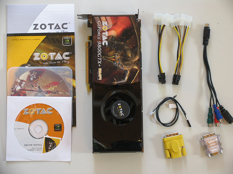
You will receive:
- Graphics card
- Manual + Driver CD + XIII Century Death or Glory full game
- DVI Adapter + HDMI Adapter
- 2x PCI-Express power adapter
- TV out cable
- SPDIF audio cable
The Card


Other than the little plus on the sticker, the GeForce 9800 GTX+ looks identical to the 9800 GTX in every aspect. Just like its predecessor it uses a dual slot cooling solution that looks very stylish thanks to the curved surface.

The card has two DVI ports, basically the most common output configuration these days. In case you need an analog VGA port you can use the included DVI adapter. When using an HDMI adapter (also included), you will also have access to HDMI+HDCP+Audio, which allows easy setup of a media PC. For the HDMI audio feature you have to connect the included SPDIF cable from your on-board audio or sound card to the input on the graphics card.


Here are the front and the back of the card, high-res versions are also available (front, back). If you choose to use these images for voltmods etc, please include a link back to this site or let us post your article.
A Closer Look


The cooler is unchanged from the non-plus 9800 GTX. It uses a complex base plate to cool not only the GPU core, but also the memory chips and the voltage regulation circuitry.

Just like the 9800 GTX, the 9800 GTX+ supports SLI and triple SLI.

Two six-pin PCI-Express power connectors supply the required power to the card.

The GDDR3 chips are made by Samsung and have the model number K4J52324QE-BJ08. They are rated for 1200 MHz operation (0.8 ns cycle time).


When I removed the heatsink I noticed that someone at Zotac used a bit too much thermal paste on the GPU. In the first picture the GPU die looks a bit like a meteorite that smashed into a sea of thermal paste. The second picture shows the GPU after some cleanup action. Please note the B1 label which indicates that this GPU is produced in a 55 nm process at TSMC. The G92 GPU from the old 9800 GTX is made in a 65 nm process.
To demonstrate the differences between the 65 nm and the 55 nm G92 I overlayed both die shots in Photoshop. The red borders mark the different die sizes. The dimly lit components are from the 65 nm A2 version, while the fully visible ones are from the 55 nm B2 silicon.
Our Patreon Silver Supporters can read articles in single-page format.
Nov 15th, 2026 16:32 CST
change timezone
Latest GPU Drivers
New Forum Posts
- What are you playing? (26222)
- WarpCoreBench scores! (51)
- Asus Rog Maximus Z890 Extreme. (Various questions). (25)
- Power supply noise stops when I move the mouse (9)
- TPU's Nostalgic Hardware Club (22165)
- HP Office Jet 7740 Pro - Supply system problem with replacement cartridge (3)
- Recommendations Wanted - Affordable Enterprise SSD for Boot (9)
- Folding Pie and Milestones!! (10204)
- What can the FX 8320 do today? Here is the answer. (59)
- How do you get games for PC? (59)
Popular Reviews
- AMD Zen 6 Technical Deep Dive
- ASUS ROG Strix B850-I Gaming Wi-Fi7 W Review
- Corsair HX1000i Shift Crystal Review
- Upcoming Hardware Launches 2027 (Updated Nov 2026)
- Montech King 95 3D PRO Review
- NZXT C1200 Platinum Review
- NZXT H7 RGB+ Review
- NZXT H5 Review
- Phantom Blade Zero Performance Benchmark Review - 35 GPUs Tested
- AMD Ryzen 7 9800X3D Review - The Best Gaming Processor
TPU on YouTube
Controversial News Posts
- NVIDIA Co-Founder and CEO Jensen Huang Officially Resigns (421)
- Open Letter Asking NVIDIA to Reinstate Jensen Huang Passes 115,000 Signatures (184)
- OpenAI CEO Argues Home PCs Waste the World's Limited DRAM Supply (152)
- NVIDIA Launches Investigation Into Jensen Huang's Relationship With Suspected Chinese Spy (136)
- Intel "Raptor Lake Next" 16-Core and 20-Core CPUs Surface (130)
- Legendary Game Studio BioWare Shuts Down Following EA Layoffs (104)
- Dell CEO Says the Memory Shortage Will Get Worse in 2027 (95)
- NVIDIA GeForce RTX 50-Series Scheduled for up to $500 Price Hike This Week (89)