 7
7
Zotac GeForce RTX 3060 AMP White Edition Review
Pictures & Teardown »The GeForce Ampere Architecture
Last year, we did a comprehensive article on the NVIDIA GeForce Ampere graphics architecture, along with a deep-dive into the key 2nd Gen RTX technology and various other features NVIDIA is introducing that are relevant to gaming. Be sure to check out that article for more details.

The GeForce Ampere architecture is the first time NVIDIA both converged and diverged its architecture IP between graphics and compute processors. Back in May, NVIDIA debuted Ampere on its A100 Tensor Core compute processor targeted at AI and HPC markets. The A100 Tensor Core is a headless compute chip that lacks all raster graphics components, so NVIDIA could cram in the things relevant to the segment. The GeForce Ampere, however, is a divergence with a redesigned streaming multiprocessor different from that of the A100. These chips have all the raster graphics hardware, display and media acceleration engines, and, most importantly, 2nd generation RT core that accelerates real-time raytracing. A slightly slimmed down version of the 3rd generation tensor core of the A100 also gets carried over. NVIDIA sticks to using GDDR-type memory over expensive memory architectures, such as HBM2E.
NVIDIA pioneered real-time raytracing on consumer graphics hardware, and three key components make the NVIDIA RTX technology work: the SIMD components, aka CUDA cores, the RT cores, which do the heavy lifting with raytracing, calculating BVH traversal and intersections, and tensor cores, which are hardware components accelerating AI deep-learning neural net building and training. NVIDIA uses an AI-based denoiser for RTX. With Ampere, NVIDIA is introducing new generations of the three components, with the objective being to reduce the performance cost of RTX and nearly double performance over generations. These include the new Ampere streaming multiprocessor that more than doubles FP32 throughput over generations, the 2nd Gen RT core that features hardware that enables new RTX effects, such as raytraced motion blur, and the 3rd generation tensor core, which leverages sparsity in DNNs to increase AI inference performance by an order of magnitude.
GA106 GPU and Ampere SM
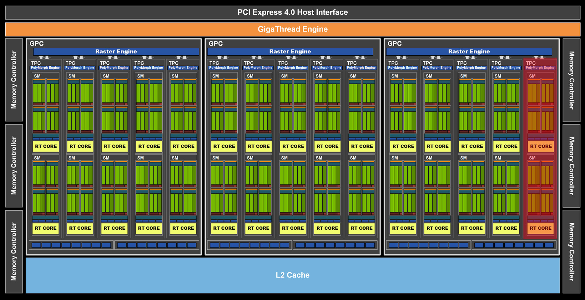
The GeForce RTX 3060 debuts NVIDIA's smallest GeForce "Ampere" GPU launched thus far, the "GA106." A successor to the "TU106" from the previous generation, the "GA106" is expected to power the midrange of this generation, with several upcoming SKUs besides the RTX 3060. It's also extensively used in the company's RTX 30-series Mobile graphics family. The "GA106" is built on the same 8 nm silicon fabrication node by Samsung as the rest of the GeForce "Ampere" family. Its die measures 276 mm² and crams in 13.25 billion transistors.
The GA106 silicon features a largely similar component hierarchy to past-generation NVIDIA GPUs, but with the bulk of engineering effort focused on the new Ampere Streaming Multiprocessor (SM). The GPU supports the PCI-Express 4.0 x16 host interface, which doubles the host interface bandwidth over PCI-Express 3.0 x16. NVIDIA has doubled the memory amount over the previous-generation RTX 2060, to 12 GB. The memory bus width is unchanged at 192-bit GDDR6. There's a slight uptick in memory clock, which now runs at 15 Gbps (GDDR6-effective), working out to 360 GB/s memory bandwidth, as opposed to 336 GB/s on the RTX 2060.
The GA106 silicon features three graphics processing clusters (GPCs), the mostly independent subunits of the GPU. Each GPC has five texture processing clusters (TPCs), the indivisible subunit that is the main number-crunching muscle of the GPU. One random TPC is disabled to carve out the RTX 3060. Each TPC shares a PolyMorph engine between two streaming multiprocessors (SMs). The SM is what defines the generation and where the majority of NVIDIA's engineering effort is localized. The Ampere SM crams in 128 CUDA cores, double that of the 64 CUDA cores in the Turing SM. The GeForce RTX 3060 hence ends up with 14 TPCs, 28 streaming multiprocessors, which work out to 3,584 CUDA cores. The chip features 112 Tensor cores, 28 RT cores, 112 TMUs, and 48 ROPs.


Each GeForce Ampere SM features four processing blocks that each share an L1I cache, warp scheduler, and a register file among 128 CUDA cores. From these, 64 can handle concurrent FP32 and INT32 math operations, while 64 are pure FP32. Each cluster also features a 3rd generation Tensor Core. At the SM level, the four processing blocks share a 128 KB L1D cache that also serves as shared memory; four TMUs and a 2nd generation RT core. As we mentioned, each processing block features two FP32 data paths; one of these consists of CUDA cores that can execute 16 FP32 operations per clock cycle, while the other data path consists of CUDA cores capable of 16 FP32 and 16 INT32 concurrent operations per clock. Each SM also features a tiny, unspecified number of rudimentary FP64 cores, which work at 1/64 the performance of the FP64 cores on the A100 Tensor Core HPC processor. These FP64 cores are only there so double-precision software doesn't run into compatibility problems.
2nd Gen RT Core, 3rd Gen Tensor Core


NVIDIA's 2nd generation RTX real-time raytracing technology sees the introduction of more kinds of raytraced effects. NVIDIA's pioneering technology involves composing traditional raster 3D scenes with certain raytraced elements, such as lighting, shadows, global illumination, and reflections.


As explained in the Ampere Architecture article, NVIDIA's raytracing philosophy involves heavy bounding volume hierarchy (BVH) traversal, and bounding box/triangle intersection, for which NVIDIA developed a specialized MIMD fixed function in the RT core. Fixed-function hardware handles both the traversal and intersection of rays with bounding boxes or triangles. With the 2nd Gen RT core, NVIDIA is introducing a new component which interpolates triangle position by time. This component enables physically accurate, raytraced motion-blur. Until now, motion-blur was handled as a post-processing effect.
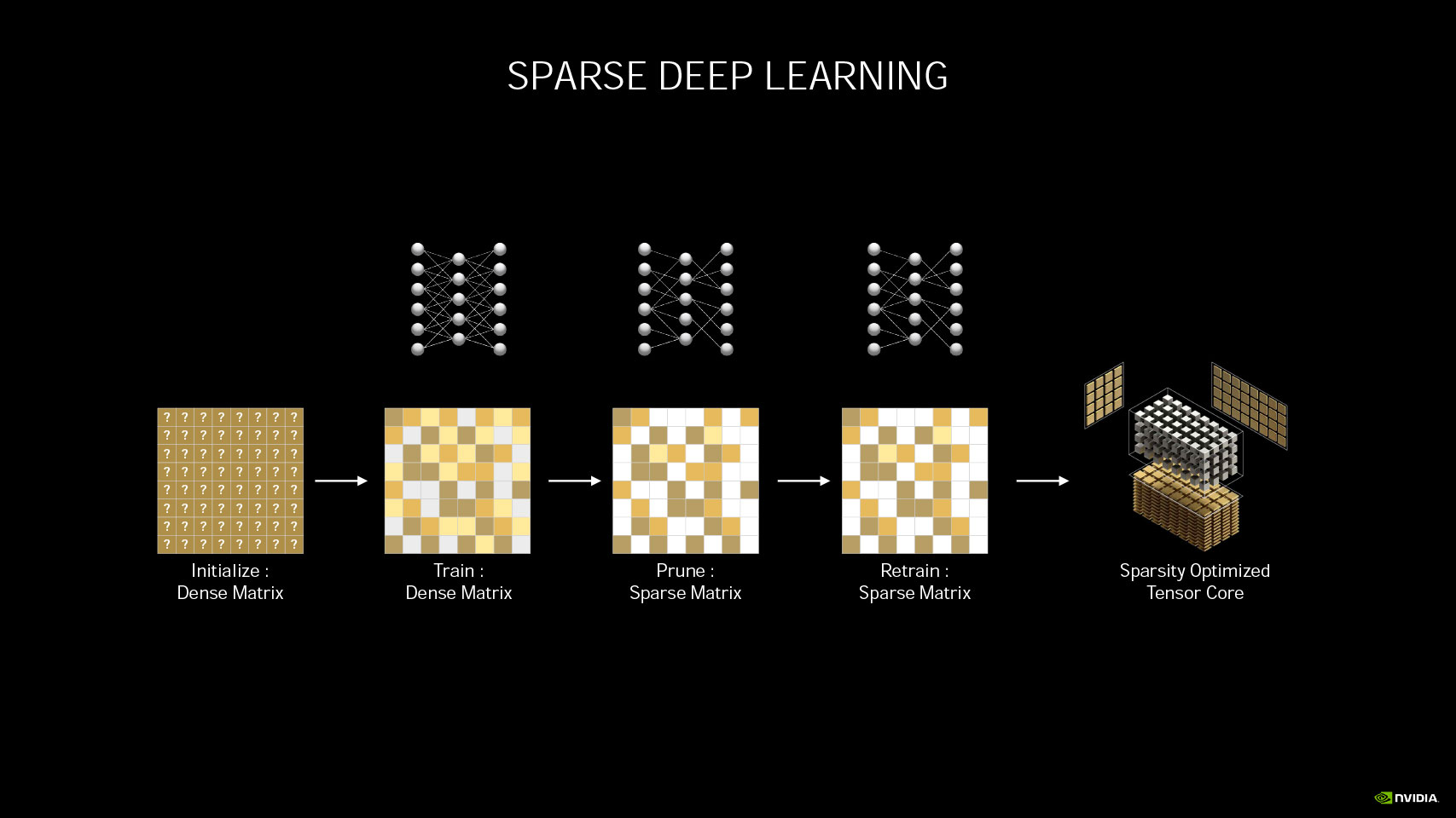

The 3rd generation tensor core sees NVIDIA build on the bulwark of its AI performance leadership, fixed-function hardware designed for tensor math which accelerates AI deep-learning neural-net building and training. AI is heavily leveraged in NVIDIA architectures now as the company uses an AI-based denoiser for its raytracing architecture and to accelerate technologies such as DLSS. Much like the 3rd generation tensor cores on the company's A100 Tensor Core processor that debuted this Spring, the new tensor cores leverage a phenomenon called sparsity—the ability for a DNN to shed its neural net without losing the integrity of its matrix. Think of this like Jenga: You pull pieces from the middle of a column while the column itself stays intact. The use of sparsity increases AI inference performance by an order of magnitude: 256 FP16 FMA operations in a sparse matrix compared to just 64 on the Turing tensor core, and 1024 sparse FP16 FMA ops per SM compared to 512 on the Turing SM, which has double the tensor core counts.
Display and Media

NVIDIA updated the display and media acceleration components of Ampere. To begin with, VirtualLink, or the USB type-C connection, has been removed from the reference design. We've seen no other custom-design cards implement it, so it's safe to assume NVIDIA junked it. The GeForce RTX 3080 puts out three DisplayPort 1.4a, which takes advantage of the new VESA DSC 1.2a compression technology to enable 8K 60 Hz with HDR using a single cable. It also enables 4K at 240 Hz with HDR. The other big development is support for HDMI 2.1, which enables 8K at 60 Hz with HDR, using the same DSC 1.2a codec. NVIDIA claims that DSC 1.2a is "virtually lossless" in quality. Except for the addition of AV1 codec hardware decode, the media acceleration features are largely carried over from Turing. As the next major codec to be deployed by the likes of YouTube and Netflix, AV1 is big. It halves the file size over H.265 HEVC for comparable quality. The new H.266 VVC misses out as the standard was introduced too late into Ampere's development.
Apr 24th, 2024 21:45 EDT
change timezone
Latest GPU Drivers
New Forum Posts
- Is there a technical reason that Windows 11 doesn't have built into it battery charge limitation? (42)
- (Anti) SFF fun house (347)
- Cinebench crashed my PC. My Wi-Fi stopped working, and I keep getting a "Please wait" screen when I boot up my PC. (30)
- The TPU UK Clubhouse (24783)
- Sharing experience with MSI RTX 3070 vBIOS update to enable Resizable Bar with MB Z490 (2)
- Share your AIDA 64 cache and memory benchmark here (2915)
- Will a RTX 4070 TI super bottleneck a Ryzen 9 7950X3D? (58)
- The best *budget* ATX PC case on the market? (24)
- GTX 1070 Ti - TDP Issues - Always Power Throttling (4)
- 2022-X58/1366 PIN Motherboards NVME M.2 SSD BIOS MOD Collection (656)
Popular Reviews
- Fractal Design Terra Review
- Thermalright Phantom Spirit 120 EVO Review
- Corsair 2000D Airflow Review
- Minisforum EliteMini UM780 XTX (AMD Ryzen 7 7840HS) Review
- ASUS GeForce RTX 4090 STRIX OC Review
- NVIDIA GeForce RTX 4090 Founders Edition Review - Impressive Performance
- ASUS GeForce RTX 4090 Matrix Platinum Review - The RTX 4090 Ti
- MSI GeForce RTX 4090 Suprim X Review
- MSI GeForce RTX 4090 Gaming X Trio Review
- Gigabyte GeForce RTX 4090 Gaming OC Review
Controversial News Posts
- Sony PlayStation 5 Pro Specifications Confirmed, Console Arrives Before Holidays (116)
- NVIDIA Points Intel Raptor Lake CPU Users to Get Help from Intel Amid System Instability Issues (106)
- AMD "Strix Halo" Zen 5 Mobile Processor Pictured: Chiplet-based, Uses 256-bit LPDDR5X (101)
- US Government Wants Nuclear Plants to Offload AI Data Center Expansion (98)
- Windows 10 Security Updates to Cost $61 After 2025, $427 by 2028 (84)
- Developers of Outpost Infinity Siege Recommend Underclocking i9-13900K and i9-14900K for Stability on Machines with RTX 4090 (84)
- TechPowerUp Hiring: Reviewers Wanted for Motherboards, Laptops, Gaming Handhelds and Prebuilt Desktops (78)
- AMD's RDNA 4 GPUs Could Stick with 18 Gbps GDDR6 Memory (73)